19
3).
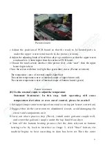
The upper sucker will go down to
(
)welding position as set in
“picture 6” to pick up the BGA chip, and goes up the Optic position set in “picture 6”
4).
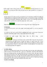
The optical CCD camera will go out right away for alignment, the BGA tin ball and
welding pad will be displayed on the monitor screen, you can check images of tin balls
on the screen through the adjusting angle handle--X axis,Y axis and angle axis,the tin
ball and PCB’s pad must be coincided completely on the screen
5)
Click the
, the monitor screen will go back to its original position.
8. Soldering
1
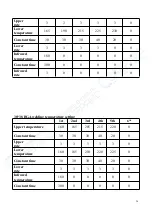
. Switch on the power, select the proper stored temp profile or set for yourself if
needed.
2
. Switch on the laser, put the BGA soldering pad center to the laser. Fasten the
supporter. Install the proper nozzle, 2mm-3mm larger than the BGA.
2. Install the right nozzle 2mm larger than the BGA chip,
click
.heating as your chosen data Cool the BGA chip after the procedure
finished Raise the upper heater to make the bottom of upper heater has 3-5mm
distance from the upper surface of BGA chip, and keep cooling for 30-40 seconds
Or you can move away the warm heater after the starting light off Then take away
the PCB board from the supporter
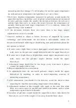
(1) Null welding:
Because of counterpoint by hand will cause deviation between chip and welding plate,
surface tension of tin ball will have a process of automatic correction between BGA
chip and welding pad Once heating, BGA falls not evenly, which will cause that the
chip drops not evenly It will cause the phenomenon of missing weld and false weld if
stop reflowing at this time, the chip will not fall normally So it is necessary for you to
extend heating time of third .forth temperature zones or add the bottom pre-heating
temperature to make the tin balls meltdown and drop evenly
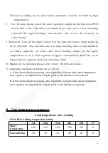
(2) short-circuiting
:


