83
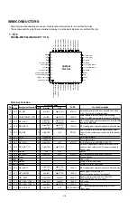
Pin
Port
Name
Assignment Function
I/O Port De
fi
nition
PU/PD
Function Description
I/O
Normal
OFF
22
P1.2 MCU_IIC_SDA
O/I
High(3.3V)
Hi-Z
4.7K PU SW3.3V
I2C Data signal that comunicate with MT8530.
(Slave mode).
23
P1.1 AC_DET
I
High(3.3V)/50Hz
or 60Hz pulse
High(3.3V)/50Hz
or 60Hz pulse
10k PU
Detection signal is for AC power.
24
P1.0 Not use
-
Hi-Z
Hi-Z
-
Not use
25
P0.7 RXD_0
I
High(3.3V)
High(3.3V)
10k PU
UART receiving terminal is from external RS232
control.
26
P0.6 TXD_0
O
High(3.3V)
High(3.3V)
10k PU
UART transmission terminal is for external RS232
control.
27
P0.5 KEY_IN_B
I
High(3.3V)
High(3.3V)
10k PU
A/D key B input signal is from key board.
28
P0.4 MCU_IR_IN
I
High(3.3V)
High(3.3V)
33k PU
IR signal input.Low is to activate the IR receiving.
29
P0.3 KEY_IN_A
I
High(3.3V)
High(3.3V)
10k PU
A/D key A input signal is from key board.
30
P0.2 MCU_SET4
I
High(3.3V)
or Low(0V)
High(3.3V)
or Low(0V)
10k PU
MCU setting pin by externail resistance. Default is high.
31
P0.1 Not use
-
Hi-Z
Hi-Z
-
Not use
32
P0.0 Standby key
I
High(3.3V)
High(3.3V)
10k PU
Power key signal input terminal.Fall-edge is valid.
33
VSS Power
-
-
-
-
Not use
34 VDD2.5 Power
-
-
-
-
Internal Regulator Output 2.5V
35
VDD Power
-
-
-
-
Supply Voltage 3.3V
36 RSTN RSTN
I
High2.5V)
Low(0V)
-
Reset Low active
37
P2.4 Not use
-
Hi-Z
Hi-Z
-
Not use
38
P2.5 Not use
-
Hi-Z
Hi-Z
-
Not use
39
P2.6 Not use
-
Hi-Z
Hi-Z
-
Not use
40
P2.7 CEC_RS232_SWITCH O
Low(0V)
High(3.3V)
10k PU
Switch singal is to switch MCU receive the singal of the
HDMI CEC and RS232. High is for MCU to receive the
signal of HDMI CEC and low is for switch those singal
input to MT8530.
41
P3.0 Not use
-
Hi-Z
Hi-Z
-
Not use
42
P3.1 AMX_POWER
O
High(3.3V)
Hi-Z
10k PD
Power enable is for RS232C circuit power supply. It is
high in power-on and normal standby mode.Low is in
STOP standby mode.
43
P3.2 Not use
-
Hi-Z
Hi-Z
-
Not use
44
P3.3 Not use
-
Hi-Z
Hi-Z
-
Not use
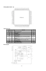
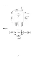
Block Diagram
1-CYCLE
8051
CPU CORE
2KB SRAM
FLASH CONTROLLER
32KB
FLASH MEMORY
POWER
MANAGER
LVD/LVR
RESET
IOSC
CLOCK
SELECT
WDT
XOSC
RTC
INTERRUPT
PORT0/1/2/3/4
UART-0
PCA
ADC
TIMER0/1/2
IO MULTIPLEXER
VDD
VSS
RSTN
SPI
UART-1
I2C Master/Slave
I2C Slave
VDD25
CEC ENGINE
PGAs
PORT0 [7:0]
PORT1 [7:0]
PORT2 [7:0]
PORT3 [7:0]
PORT4 [7:0]
IO
MU
LTIPL
E
XER
Analog
Comparators
Analog Switches
Содержание DBP-2012UDCI
Страница 17: ...17 5 On the screen below select ComPort XX Select the USB 232C TTL conversion jig port 6 Check Directory ...
Страница 40: ...40 Personal notes ...
Страница 76: ...Personal notes Personal notes 76 ...
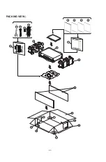
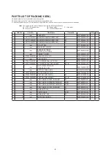
Страница 80: ...80 PACKING VIEWs 7 8 8 14 15 16 17 19 18 17 16 19 9 13 12 11 10 z 1 3 4 5 6 ...
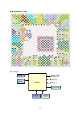
Страница 86: ...86 LAN8710 MAIN UNIT U901 Block Diagram ...
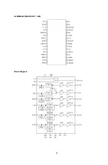
Страница 87: ...87 NJM2566AV MAIN UNIT U20 Block Diagram ...
Страница 91: ...91 2 FL DISPLAY FL TUBE 15 BT 114GNK Display UNIT U3 ...
Страница 92: ...92 Personal notes ...


