


© Cobham Gaisler AB
Kungsgatan 12 | SE-411 19 Goteborg | Sweden
+46 31 7758650 | www.caes.com/gaisler
11
GR-CPCIS-XCKU
Document Data Sheet & User Manual
Feb 2022, Version 1.2
GTH banks Q126, Q127, Q128 are unused on this board.
4.4
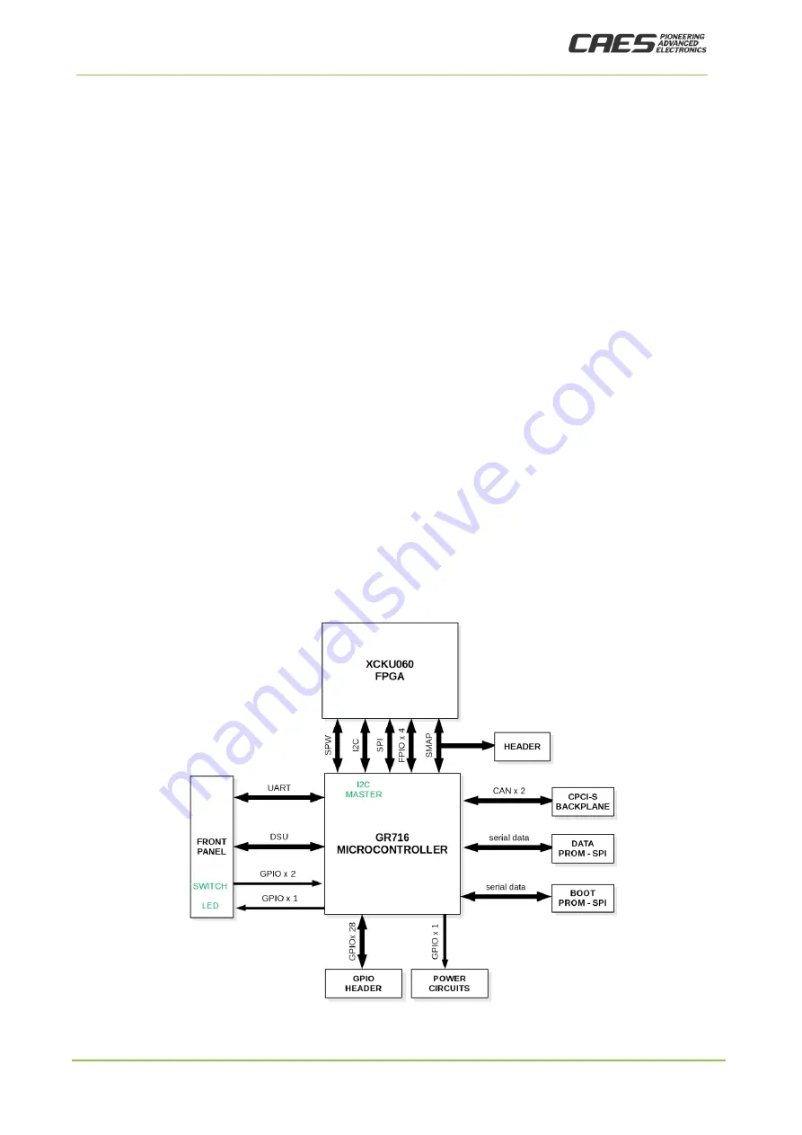
GR716 Microcontroller
The microcontroller has the following interfaces as represented in Figure 5.
SMAP
Parallel data interface for read-out and programming of FPGA configuration.
I2C
Two-wire Serial I2C interface with GR716 as Master (see section 4.6.6)
SPI
SPI master interface for user-defined SPI data exchange with FPGA
FPIO[3..0]
Four 3.3V LVTTL signals for user defined signalling between GR716 and FPGA
SPW
Spacewire LVDS interface between GR716 and FPGA
CAN3
CAN data interface between GR716 and Backplane
CAN4
CAN data interface between GR716 and Backplane
SPI-BOOT SPI Memory interface to Serial SPI memory (see section 4.5)
SPI-DATA SPI Memory interface to Serial SPI memory (see section 4.5)
UART2
2-wire Serial UART interface to GR716 UART0 interface
DSU
2-wire Serial UART interface to GR716 Debug Support Unit interface
GR-STS
GPIO output connected to front-panel LED for user defined signalling
GR-EN
Front panel DIP Switch connected to GR716 DSU Enable input
GR-BRE
Front panel DIP Switch connected to GR716 DSU Break input
GPIO-HDR28 GPIO signals for GR716 connected to standard 0.1” header for user defined purposes
FMC-ON
GPIO to Power Circuits to control the enabling of the +12V FMC power supply
Figure 5
GR716 Interfaces