ATtiny22/22L
41
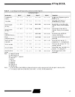
Note:
a = address high bits
b = address low bits
H = 0 - Low byte, 1- High byte
o = data out
i = data in
x = don’t care
1 = lock bit 1
2 = lock bit 2
R = RCEN Fuse
S = SPIEN Fuse
Notes:
1. When the state of the RCEN bit is changed, the device must be power cycled for the changes to have any effect.
2. The signature bytes are not readable in Lock mode 3, i.e. both Lock bits programmed.
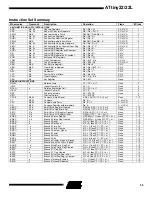
Table 17. Low-Voltage Serial Programming Instruction Set ATtiny22/L
Instruction
Instruction Format
Operation
Byte 1
Byte 2
Byte 3
Byte 4
Programming
Enable
1010 1100
0101 0011
xxxx xxxx
xxxx xxxx
Enable Serial Programming while
RESET is low.
Chip Erase
1010 1100
100x xxxx
xxxx xxxx
xxxx xxxx
Chip erase both Flash and
EEPROM memory arrays.
Read Program
Memory
0010 H000
0000 00aa
bbbb bbbb
oooo oooo
Read H (high or low) data o from
Program memory at word address
a:b.
Write Program
Memory
0100 H000
0000 00aa
bbbb bbbb
iiii iiii
Write H (high or low) data i to
Program memory at word address
a:b.
Read
EEPROM Memory
1010 0000
0000 0000
xbbb bbbb
oooo oooo
Read data o from EEPROM
memory at address b.
Write
EEPROM Memory
1100 0000
0000 0000
xbbb bbbb
iiii iiii
Write data i to EEPROM memory at
address b.
Read Lock and
Fuse Bits
0101 1000
xxxx xxxx
xxxx xxxx
12Sx xxxR
Read Lock and Fuse bits. ‘0’ =
programmed, ‘1’ = unprogrammed.
Write Lock Bits
1010 1100
1111 1
211
xxxx xxxx
xxxx xxxx
Write Lock bits. Set bits
1,2 = ‘0’ to
program Lock bits.
Write RCEN Bit
1010 1100
1011 111R
xxxx xxxx
xxxx xxxx
Write RCEN Fuse. Set bit R = ‘0’ to
program, ‘1’ to unprogram.
Read Signature
Bytes
0011 0000
xxxx xxxx
xxxx xxbb
oooo oooo
Read Signature byte o from
address b


