ATtiny22/22L
44
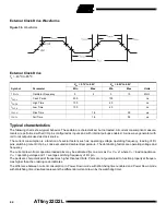
External Clock Drive Waveforms
Figure 36. Waveforms
External Clock Drive
T
A
= -40
°
C to 85
°
C
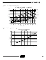
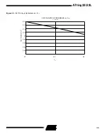
Typical characteristics
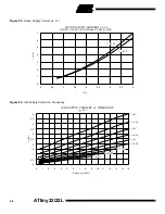
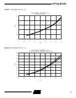
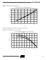
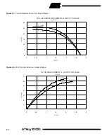
The following charts show typical behavior. These data are characterized, but not tested. All current consumption measure-
ments are performed with all I/O pins configured as inputs and with internal pull-ups enabled. A sine wave generator with
rail to rail output is used as clock source.
The current consumption is a function of several factors such as: operating voltage, operating frequency, loading of I/O
pins, switching rate of I/O pins, code executed and ambient temperature. The dominating factors are operating voltage and
frequency.
The current drawn from capacitive loaded pins may be estimated (for one pin) as C
L
x
V
CC
x f where C
L
= load capacitance,
V
CC
= operating voltage and f = average switching frequency of I/O pin.
The parts are characterized at frequencies higher than test limits. Parts are not guaranteed to function properly at frequen-
cies higher than the ordering code indicates.
The difference between current consumption in Power Down mode with Watchdog timer enabled and Power Down mode
with Watchdog timer disabled represents the differential current drawn by the watchdog timer.
Symbol
Parameter
V
CC
= 2.7V to 4.0V
V
CC
= 4.0V to 6.0V
Units
Min
Max
Min
Max
1/t
CLCL
Oscillator Frequency
0
4
0
10
MHz
t
CLCL
Clock Period
250
100
ns
t
CHCX
High Time
100
40
ns
t
CLCX
Low Time
100
40
ns
t
CLCH
Rise Time
1.6
0.5
µs
t
CHCL
Fall Time
1.6
0.5
µs
VIL1
VIH1


