background image

22

ATtiny22/22L

MCU Status Register - MCUSR

The MCU Status Register provides information on which reset source caused a MCU reset:

Bit 7..2 - Res: Reserved Bits

These bits are reserved bits in the ATtiny22/L and always read as zero.

Bit 1 - EXTRF: External Reset Flag

After a power-on reset, this bit is undefined (X). It will be set by an external reset. A watchdog reset will leave this bit
unchanged.

Bit 0 - PORF: Power-On Reset Flag

This bit is set by a power-on reset. A watchdog reset or an external reset will leave this bit unchanged.

To summarize, the following table shows the value of these two bits after the three modes of reset.

To make use of these bits to identify a reset condition, the user software should clear both the PORF and EXTRF bits as
early as possible in the program. Checking the PORF and EXTRF values is done before the bits are cleared. If the bit is
cleared before an external or watchdog reset occurs, the source of reset can be found by using the following truth table:

Interrupt Handling

The ATtiny22/L has two 8-bit Interrupt Mask control registers; GIMSK - General Interrupt Mask register and TIMSK -
Timer/Counter Interrupt Mask register.

When an interrupt occurs, the Global Interrupt Enable I-bit is cleared (zero) and all interrupts are disabled. The user
software can set (one) the I-bit to enable nested interrupts. The I-bit is set (one) when a Return from Interrupt instruction -
RETI - is executed.

When the Program Counter is vectored to the actual interrupt vector in order to execute the interrupt handling routine, hard-
ware clears the corresponding flag that generated the interrupt. Some of the interrupt flags can also be cleared by writing a
logic one to the flag bit position(s) to be cleared.

If an interrupt condition occurs when the corresponding interrupt enable bit is cleared (zero), the interrupt flag will be set
and remembered until the interrupt is enabled, or the flag is cleared by software.

If one or more interrupt conditions occur when the global interrupt enable bit is cleared (zero), the corresponding interrupt
flag(s) will be set and remembered until the global interrupt enable bit is set (one), and will be executed by order of priority.

Note that external level interrupt does not have a flag, and will only be remembered for as long as the interrupt condition is
active.

Bit

7

6

5

4

3

2

1

0

$34  ($54)

-

-

-

-

-

-

EXTRF

PORF

MCUSR

Read/Write

R

R

R

R

R

R

R/W

R/W

Initial value

0

0

0

0

0

0

See bit description

Table 5.  PORF and EXTRF Values after Reset

Reset Source

PORF

EXTRF

Power-On Reset

1

undefined

External Reset

unchanged

1

Watchdog Reset

unchanged

unchanged

Table 6.  Reset Source Identification

PORF

EXTRF

Reset Source

0

0

Watchdog Reset

0

1

External Reset

1

0

Power-On Reset

1

1

Power-On Reset

Содержание AVR ATtiny22

Страница 1: ...l and Internal Interrupt Sources Power on Reset Circuit Selectable On chip RC Oscillator Specifications Low power High speed CMOS Process Technology Fully Static Operation Power Consumption at 4 MHz 3...

Страница 2: ...cient while achieving throughputs up to ten times faster than conventional CISC microcontrollers Block Diagram Figure 1 The ATtiny22 L Block Diagram PROGRAM COUNTER INTERNAL OSCILLATOR WATCHDOG TIMER...

Страница 3: ...to many embedded control applications The ATtiny22 L AVR is supported with a full suite of program and system development tools including C compilers macro assemblers program debugger simulators in ci...

Страница 4: ...16 bit indirect address register pointers for Data Space addressing enabling efficient address calculations One of the three address pointers is also used as the address pointer for the constant table...

Страница 5: ...truction is being executed the next instruction is pre fetched from the program memory This concept enables instructions to be executed in every clock cycle The program memory is in system downloadabl...

Страница 6: ...tions SBCI SUBI CPI ANDI ORI between a constant and a register and the LDI instruction for load immediate constant data These instructions apply to the second half of the regis ters in the register fi...

Страница 7: ...System Programmable Flash memory for program storage Since all instruc tions are 16 or 32 bit words the Flash is organized as 1K x 16 The Flash memory has an endurance of at least 1000 write erase cyc...

Страница 8: ...R31 feature the indirect addressing pointer registers The Direct addressing reaches the entire data address space The Indirect with Displacement mode features 63 address locations reach from the base...

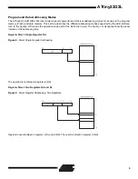
Страница 9: ...AVR architec ture In the figures OP means the operation code part of the instruction word To simplify not all figures show the exact location of the addressing bits Register Direct Single Register Rd...

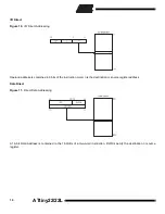
Страница 10: ...ress is contained in 6 bits of the instruction word n is the destination or source register address Data Direct Figure 11 Direct Data Addressing A 16 bit Data Address is contained in the 16 LSBs of a...

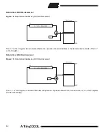
Страница 11: ...Indirect with Displacement Operand address is the result of the Y or Z register contents added to the address contained in 6 bits of the instruction word Data Indirect Figure 13 Data Indirect Addressi...

Страница 12: ...remented before the operation Operand address is the decremented contents of the X Y or the Z register Data Indirect With Post Increment Figure 15 Data Indirect Addressing With Post Increment The X Y...

Страница 13: ...the Z register contents The 15 MSBs select word address 0 1K the LSB selects low byte if cleared LSB 0 or high byte if set LSB 1 Indirect Program Addressing IJMP and ICALL Figure 17 Indirect Program...

Страница 14: ...ied to the CLOCK pin No internal clock division is used Figure 19 The Parallel Instruction Fetches and Instruction Executions Figure 19 shows the parallel instruction fetches and instruction execution...

Страница 15: ...ecuted and the result is stored back to the destination register Figure 21 On Chip Data SRAM Access Cycles The internal data SRAM access is performed in two System Clock cycles as described in Figure...

Страница 16: ...status flags are cleared by writing a logical one to them Note that the CBI and SBI instructions will operate on all bits in the I O register writing a one back into any flag read as set thus clearing...

Страница 17: ...an arithmetical or logical operation See the Instruction Set Description for detailed information Bit 1 Z Zero Flag The zero flag Z indicates a zero result from an arithmetical or logical operation S...

Страница 18: ...threshold VPOT External Reset The MCU is reset when a low level is present on the RESET pin for more than 50 ns Watchdog Reset The MCU is reset when the Watchdog timer period expires and the Watchdog...

Страница 19: ...uency The start up time tTOUT is one watchdog cycle The frequency of the watchdog oscillator is voltage dependent as shown in Typical characteristics on page 44 Table 3 Reset Characteristics VCC 5 0V...

Страница 20: ...Ttiny22 22L Figure 23 MCU Start Up RESET Tied to VCC Figure 24 MCU Start Up RESET Controlled Externally VCC RESET TIME OUT INTERNAL RESET tTOUT VPOT VRST VCC RESET TIME OUT INTERNAL RESET tTOUT VPOT V...

Страница 21: ...he Reset Threshold Voltage VRST on its positive edge the delay timer starts the MCU after the Time out period tTOUT has expired Figure 25 External Reset During Operation Watchdog Reset When the Watchd...
Страница 22: ...led The user software can set one the I bit to enable nested interrupts The I bit is set one when a Return from Interrupt instruction RETI is executed When the Program Counter is vectored to the actua...

Страница 23: ...t 6 INTF0 External Interrupt Flag0 When an event on the INT0 pin triggers an interrupt request INTF0 becomes set one If the I bit in SREG and the INT0 bit in GIMSK are set one the MCU will jump to the...

Страница 24: ...4 clock cycles after the interrupt flag has been set the program vector address for the actual interrupt handling routine is executed During these 4 clock cycles the Program Counter 2 bytes is popped...

Страница 25: ...ared zero the SLEEP instruction forces the MCU into the Idle Mode stopping the CPU but allowing Timer Counters Watchdog and the interrupt system to continue operating This enables the MCU to wake up f...

Страница 26: ...the Timer Counter0 Control Register TCCR0 The overflow status flag is found in the Timer Counter Interrupt Flag Register TIFR Control signals are found in the Timer Counter0 Control Register TCCR0 Th...

Страница 27: ...Bit 2 1 and 0 The Clock Select0 bits 2 1 and 0 define the prescaling source of Timer0 Bit 7 6 5 4 3 2 1 0 33 53 CS02 CS01 CS00 TCCR0 Read Write R R R R R R W R W R W Initial value 0 0 0 0 0 0 0 0 Tab...

Страница 28: ...data for typical values at other VCC levels The WDR Watchdog Reset instruction resets the Watchdog Timer Eight different clock cycle periods can be selected to determine the reset period If the reset...

Страница 29: ...1 WDP0 Watchdog Timer Prescaler 1 and 0 The WDP2 WDP1 and WDP0 bits determine the Watchdog Timer prescaling when the Watchdog Timer is enabled The different prescaling values and their corresponding t...

Страница 30: ...ess given by EEAR EEPROM Control Register EECR Bit 7 3 Res Reserved Bits These bits are reserved bits in the ATtiny22 L and will always read as zero Bit 2 EEMWE EEPROM Master Write Enable The EEMWE bi...

Страница 31: ...ould poll the EEWE bit before starting the read operation If a write operation is in progress when new data or address is written to the EEPROM I O registers the write operation will be interrupted an...

Страница 32: ...pins with alternate functions are shown in the following table When the pins are used for the alternate function the DDRB and PORTB register has to be set according to the alternate function descripti...

Страница 33: ...grammed an external clock source must be connected to CLOCK SCK T0 Port B Bit 2 In serial programming mode this bit serves as the serial clock input SCK During normal operation this pin can serve as t...

Страница 34: ...06 Indicates ATtiny22 L when signature byte 001 is 91 Note 1 When both lock bits are programmed Lock mode 3 the signature bytes can not be read in the Low voltage Serial mode Reading the signature by...

Страница 35: ...programmed one byte at a time by supplying first the address then the low and high data byte The write instruction is self timed wait until the PB2 RDY BSY pin goes high 3 The EEPROM array is program...

Страница 36: ...0_0000_0000_00 Wait after Instr 3 until PB2 goes high Repeat Instr 1 Instr 2 and Instr 3 for each new address Read Flash High and Low Address PB0 PB1 PB2 0_0000_0010_00 0_0100_1100_00 x_xxxx_xxxx_xx...

Страница 37: ...00 0_0100_1100_00 x_xxxx_xxxx_xx 0_1111_1211_00 0_0010_1100_00 x_xxxx_xxxx_xx 0_0000_0000_00 0_0110_0100_00 x_xxxx_xxxx_xx 0_0000_0000_00 0_0110_1100_00 0_0000_0000_00 Wait after Instr 4 until PB2 goe...

Страница 38: ...rays have separate address spaces 0000 to 03FF for Flash Program memory and 000 to 07F for EEPROM Data memory Either an external clock is applied to the XTAL1 PB3 pin or the device must be clocked fro...

Страница 39: ...the second byte 53 will echo back when issuing the third byte of the Programming Enable instruction Whether the echo is correct or not all 4 bytes of the instruction must be transmitted If the 53 did...

Страница 40: ...ant to contain FF can be skipped This does not apply if the EEPROM is reprogrammed without first chip erasing the device Data Polling Flash When a byte is being programmed into the Flash reading the a...

Страница 41: ...arrays Read Program Memory 0010 H000 0000 00aa bbbb bbbb oooo oooo Read H high or low data o from Program memory at word address a b Write Program Memory 0100 H000 0000 00aa bbbb bbbb iiii iiii Write...

Страница 42: ...llator Frequency VCC 4 0 6 0V 0 8 MHz tCLCL Oscillator Period VCC 4 0 6 0V 125 ns tSHSL SCK Pulse Width High 2 tCLCL ns tSLSH SCK Pulse Width Low 2 tCLCL ns tOVSH MOSI Setup to SCK High tCLCL ns tSHOX...

Страница 43: ...rage Temperature 65 C to 150 C Voltage on any Pin except RESET with respect to Ground 1 0V to VCC 0 5V Voltage on RESET with respect to Ground 1 0V to 13 0V Maximum Operating Voltage 6 6V DC Current p...

Страница 44: ...voltage and frequency The current drawn from capacitive loaded pins may be estimated for one pin as CL x VCC x f where CL load capacitance VCC operating voltage and f average switching frequency of I...

Страница 45: ...00 14 00 16 00 18 00 20 00 0 1 2 3 4 5 6 7 8 9 10 11 12 13 14 15 ACTIVE SUPPLY CURRENT vs FREQUENCY T 25 C A Vcc 6V Vcc 5 5V Vcc 5V Vcc 4 5V Vcc 4V Vcc 3 6V Vcc 3 3V Vcc 3 0V Vcc 2 7V Frequency MHz I...

Страница 46: ...c DEVICE CLOCKED BY INTERNAL RC OSCILLATOR I cc mA Vcc V 0 1 2 3 4 5 6 7 2 2 5 3 3 5 4 4 5 5 5 5 6 T 25 C A T 85 C A 0 0 5 1 1 5 2 2 5 3 3 5 4 4 5 5 0 1 2 3 4 5 6 7 8 9 10 11 12 13 14 15 Vcc 6V Vcc 5...

Страница 47: ...s VCC 0 0 5 1 1 5 2 2 5 2 2 5 3 3 5 4 4 5 5 5 5 6 T 25 C A T 85 C A IDLE SUPPLY CURRENT vs Vcc I cc mA Vcc V FREQUENCY 4 MHz 0 0 1 0 2 0 3 0 4 0 5 0 6 0 7 0 8 2 2 5 3 3 5 4 4 5 5 5 5 6 T 25 C A T 85 C...

Страница 48: ...s VCC T 85 C A T 25 C A POWER DOWN SUPPLY CURRENT vs Vcc I cc Vcc V WATCHDOG TIMER DISABLED T 45 C A T 70 C A 0 5 10 15 20 25 2 2 5 3 3 5 4 4 5 5 5 5 6 0 20 40 60 80 100 120 140 160 180 2 2 5 3 3 5 4...

Страница 49: ...a time Figure 46 Pull Up Resistor Current vs Input Voltage 0 200 400 600 800 1000 1200 1400 1600 2 2 5 3 3 5 4 4 5 5 5 5 6 T 85 C A T 25 C A WATCHDOG OSCILLATOR FREQUENCY vs Vcc V V cc F KHz RC 0 20...

Страница 50: ...Pin Sink Current vs Output Voltage 0 5 10 15 20 25 30 0 0 5 1 1 5 2 2 5 3 PULL UP RESISTOR CURRENT vs INPUT VOLTAGE I A OP V V OP V 2 7V cc T 85 C A T 25 C A 0 10 20 30 40 50 60 70 0 0 5 1 1 5 2 2 5...

Страница 51: ...Sink Current vs Output Voltage 0 2 4 6 8 10 12 14 16 18 20 0 0 5 1 1 5 2 2 5 3 3 5 4 4 5 5 I O PIN SOURCE CURRENT vs OUTPUT VOLTAGE V 5V cc I mA OH V V OH T 85 C A T 25 C A 0 5 10 15 20 25 0 0 5 1 1 5...

Страница 52: ...igure 52 I O Pin Input Threshold Voltage vs VCC 0 1 2 3 4 5 6 0 0 5 1 1 5 2 2 5 3 I O PIN SOURCE CURRENT vs OUTPUT VOLTAGE I mA OH V V OH T 85 C A T 25 C A V 2 7V cc 0 0 5 1 1 5 2 2 5 2 7 4 0 5 0 Thre...

Страница 53: ...ATtiny22 22L 53 Figure 53 I O Pin Input Hysteresis vs VCC 0 0 02 0 04 0 06 0 08 0 1 0 12 0 14 0 16 0 18 2 7 4 0 5 0 Input hysteresis V Vcc I O PIN INPUT HYSTERESIS vs Vcc T 25 C A...

Страница 54: ...0 page 23 39 59 TIMSK TOIE0 page 15 38 58 TIFR TOV0 page 16 37 57 Reserved 36 56 Reserved 35 55 MCUCR SE SM ISC01 ISC00 page 16 34 54 MCUSR EXTRF PORF page 14 33 53 TCCR0 CS02 CS01 CS00 page 27 32 52...

Страница 55: ...f Rd Rr PC PC 2 or 3 None 1 2 CP Rd Rr Compare Rd Rr Z N V C H 1 CPC Rd Rr Compare with Carry Rd Rr C Z N V C H 1 CPI Rd K Compare Register with Immediate Rd K Z N V C H 1 SBRC Rr b Skip if Bit in Reg...

Страница 56: ...P None 1 OUT P Rr Out Port P Rr None 1 PUSH Rr Push Register on Stack STACK Rr None 2 POP Rd Pop Register from Stack Rd STACK None 2 BIT AND BIT TEST INSTRUCTIONS SBI P b Set Bit in I O Register I O P...

Страница 57: ...z Ordering Code Package Operation Range 2 7 6 0V 4 ATtiny22L 4PC ATtiny22L 4SC 8P3 8S2 Commercial 0 C to 70 C ATtiny22L 4PI ATtiny22L 4SI 8P3 8S2 Industrial 40 C to 85 C 4 0 6 0V 8 ATtiny22 8PC ATtiny...

Страница 58: ...0 7 62 0 15 REF 430 10 9 MAX 012 305 008 203 020 508 012 305 213 5 41 205 5 21 330 8 38 300 7 62 PIN 1 050 1 27 BSC 212 5 38 203 5 16 080 2 03 070 1 78 013 330 004 102 0 8 REF 010 254 007 178 035 889...

Страница 59: ...arters 2325 Orchard Parkway San Jose CA 95131 TEL 408 441 0311 FAX 408 487 2600 Europe Atmel U K Ltd Coliseum Business Centre Riverside Way Camberley Surrey GU15 3YL England TEL 44 1276 686 677 FAX 44...

Отзывы: