


AD9361 Reference Manual
UG-570
| Page 97 of 128
SINGLE PORT FULL DUPLEX MODE (CMOS)
Single port full duplex mode is used in applications requiring
FDD operation and data rates less than 30.72 MHz. In this
mode, the bus is split in half with six bits dedicated to Rx data
and six bits dedicated to Tx data. This mode can be used with
all receiver-transmitter configurations. The bus can be operated
as either SDR or DDR in this configuration. In this example,
only P0 is enabled and the data bus is split into separate subbuses.
Each sub-bus operates simultaneously allowing full duplex of
transmit and receive data between the BBP and the
AD9361
.
Because the bus must complete twice as many data transfers for
full duplex mode, the data bus must operate at twice the speed
of the TDD mode to achieve the same transmit and receive data
rates (as each are running concurrently in full duplex).
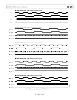
Figure 67 illustrates the connections between the
AD9361
and
the BBP for this mode of operation.
Transmit data is driven on P0_D[11:6] by the BBP such that the
setup and hold times between FB_CLK and P0_D[11:6] allow
the
AD9361
to use FB_CLK to capture the data. Receive data is
driven on P0_D[5:0] by the
AD9361
such that the setup and
hold times between DATA_CLK and P0_D[5:0] arriving at the
BBP enable the BBP to use DATA_CLK to capture the data. A
pulse on the ENABLE pin (or a rising edge) triggers the
beginning of data transfer, and another pulse (or falling edge)
signifies the end of data transfer.
The Rx_FRAME and Tx_FRAME signals indicate the
beginning of a set (frame) of data samples. The Rx_FRAME
signal can be set to occur once at the beginning of the burst
(one high transition only) for each data transfer or to have a
rising edge at the beginning of each frame and repeat with a
50% duty cycle until the data transfer is complete. Similarly,
Tx_FRAME accepts either format from the BBP.
The transmit data samples are carried in two’s complement
format, with the first 6-bit byte (P0_D[11:6]) containing the
MSBs and the second 6-bit byte (P0_D[11:6]) containing the
LSBs. P0_D[11] is the numerically most significant bit and
P0_D[6] is the least significant bit. The receive data samples are
also carried in two’s complement format, with the first 6-bit byte
(P0_D[5:0]) containing the MSB’s and the second 6-bit byte
(P0_D[5:0]) containing the LSB’s. P0_D[5] is the numerically
most significant bit and P0_D[0] is the least significant bit. In
both cases, the most positive sample value is 0x7FF, with the
first byte being 0x1F and the second byte being 0x3F. The most
negative value is 0x800, with the first byte being 0x20 and the
second byte being 0x00.
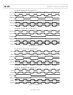
In this mode, the I and Q data samples are time-interleaved on
the data bus. For a single RF path in each direction (a 1R1T
system), the data is carried in a 4-way interleave, as follows:
I
MSB
, Q
MSB
, I
LSB
, Q
LSB
, …
For a system with two active Rx/Tx channels, the I and Q
samples from RF Channel 1 and Channel 2 are carried in an
8-way interleave, as follows:
I
1 MSB
, Q
1 MSB
, I
1 LSB
, Q
1 LSB
, I
2 MSB
, Q
2 MSB
, I
2 LSB
, Q
2 LSB
, …
For a system with a 2R1T or a 1R2T configuration, the clock
frequencies, sample periods, and data capture timing are the
same as if configured for a 2R2T system. However, in the path
with only a single channel used, the disabled channel’s I-Q pair
in each data group is unused. These unused slots are ignored by
the
AD9361
. As an example, for a 2R1T system using Transmit
Channel 1, the transmit burst would have four unused slots, as
follows:
I
1 MSB
, Q
1 MSB
, I
1 LSB
, Q
1 LSB
, X, X, X, X, …
The unused X slots can be filled with arbitrary data values by
the BBP. Such values can be constant values, or the preceding
data sample values can be repeated to reduce the bus-switching
factor and, therefore, power consumption.
Rev. A


