AD9361 Reference Manual
UG-570
| Page 111 of 128
The following bits are not supported in LVDS mode:
•
Swap Ports—In LVDS mode, P0 is Tx and P1 is Rx. This configuration cannot be changed.
•
Single Port Mode —Both ports are enabled in LVDS mode.
•
FDD Full Port—Not supported in LVDS.
•
FDD Alt Word Order—Not supported in LVDS.
•
FDD Swap Bits—Not supported in LVDS.
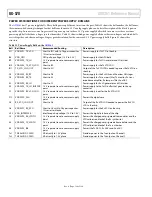
DATA PATH TIMING PARAMETERS (LVDS)
Table 51 lists the timing constraints for the LVDS data buses.
Table 51. Data Path Timing Constraint Values
—
LVDS Mode
Parameter Min
Typ
Max
Description
t
CP
4.069 ns
DATA_CLK cycle time (clock period)
t
MP
45% of t
CP
55% of t
CP
DATA_CLK and FB_CLK high and/or low minimum pulse width (including effects of duty
cycle distortion, period jitter, cycle-cycle jitter and half-period jitter)
t
STx
1 ns
Tx_D[5:0], Tx_FRAME setup time to FB_CLK falling edge at
AD9361
inputs
t
HTx
0 ns
Tx_D[5:0], Tx_FRAME hold time from FB_CLK falling edge at
AD9361
inputs
t
DDRx
0.25 ns
1.25 ns
Delay from DATA_CLK to Rx_D[5:0] outputs
t
DDDV
0.25 ns
1.25 ns
Delay from DATA_CLK to Rx_FRAME
Rev. A


