background image

ADM-XR-IIPro  User Manual 

Page 3 of 29 

Version 0.2 

Revision History 

Revision Date 

Comments 

0.1 Jul-04 

Initial 

0.1+  


DATA1, DATA8 DATA13 and DATA15 – polarity swapped 
DATA38 pin nos swapped in Manual 
Clock pins updated for XP pinouts (were XPL pinouts) 

0.2 

Nov-04 

Removed XRM-Pro Debug Section – added XRM ETH 


Содержание ADM-XRC-II Pro

Страница 1: ...ADM XR IIPro User Manual Page 1 of 29 Version 0 2 ADM XRC II Pro ADM XP Hardware Manual...

Страница 2: ...irport Parkway Suite 470 San Jose CA 95110 USA Phone 408 467 5076 Fax 408 436 5524 Email support alpha data com Copyright 2002 2003 2004 Alpha Data Parallel Systems Ltd All rights reserved This public...

Страница 3: ...Revision History Revision Date Comments 0 1 Jul 04 Initial 0 1 DATA1 DATA8 DATA13 and DATA15 polarity swapped DATA38 pin nos swapped in Manual Clock pins updated for XP pinouts were XPL pinouts 0 2 N...

Страница 4: ...PGA 10 5 1 CONFIGURATION 10 5 2 CLOCKS 10 5 3 SDRAM DDR MEMORY 12 5 4 DDR2 SSRAM 13 5 5 FLASH MEMORY 14 5 6 POWER SUPPLY 14 6 FRONT PANEL I O 15 6 1 SAMTEC 180 CONNECTOR U8 15 6 2 ROCKETIO MULTI GIGAB...

Страница 5: ...and toolkits provided by Xilinx Flexible I O is the key to the ADM XRC II series of boards and the XP is compatible with a wide selection of XRM modules that use the 180 pin Samtec interface 1 1 Speci...

Страница 6: ...is powered up The ADM XP must be secured to the PMC motherboard using M2 5 screws in the four holes provided The PMC bezel through which the I O connector protrudes should be flush with the front pan...

Страница 7: ...e bridge and the target device The bridge is capable of 66MHz PCI or PCI X operation with 64 bit or 32 bit operation The local bus supports 64 bit at upto 80Mhz The target FPGA is a Virtex II PRO devi...

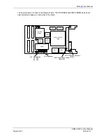
Страница 8: ...DDR DRAM and DDR2 SSRAM devices are clam shelled and appear on both sides of the board J5 Jtag Header J 1 X R M M E Z Z J 2 J 4 JP1 VIO Selection J 3 2V1500 Bridge 2VP70 2VP100 Target ZBT ZBT 1 Flash...

Страница 9: ...ignalling Virtex2Pro default 2 5V fast LVCMOS LVTTL lclk AT21 AF1 AF2 AG12 AF7 AD10 AD9 AC10 AC9 Signal Type Purpose lad 0 63 bidir Address and data bus lreset_l unidir Reset to target lads_l bidir In...

Страница 10: ...n the bridge and the target device mapped to the PCI bus This enables very rapid download of configuration data controlled by driver and API code in the host The maximum speed that can be achieved is...

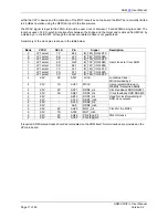
Страница 11: ...lect 6S J22 IO_74P_0 GCLK6S 0 JP1 select 5P F22 IO_75N_0 GCLK5P 0 JP1 select 4S G22 IO_75P_0 GCLK4S 1 JP1 select 0S K21 IO_74P_1 GCLK0S 1 JP1 select 1P J21 IO_74N_1 GCLK1P 1 JP1 select 2S F21 IO_75P_1...

Страница 12: ...s for data and control and SSTL1 for address and clocks Please refer to the UCF for locations of the DDR pins Please note that the FPGA requires the Vref pins to be connected for correct data receptio...

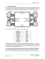
Страница 13: ...SRAM Add0 0 21 Dq0 0 31 Bwe0 0 3 Cclk0 Cclkb0 Kclk0 Kclkb0 DDR2 SSRAM Bank1 DDR2 SSRAM Bank 2 DDR2 SSRAM Bank 3 The pins required for each SSRAM controller bank are listed below Name FPGA Pin Type Des...

Страница 14: ...O standard be used for the Flash Interface 2VP70 2VP100 FF1704 dq 0 15 RC28F256K3 Strataflash K3 Flash_rst_n ad 0 23 A0 Flash_oe_n Flash_we_n Flash_cs_n VIO Bank 3 4 VCCO 2 5V VCC 2V5 3V3 Flash_wp_n F...

Страница 15: ..._8N_1 1 2 IO_35N_1 C13 E10 IO_8P_1 3 4 IO_35P_1 D13 F11 IO_19N_1 5 6 IO_30P_1 H13 E11 IO_19P_1 7 8 IO_30N_1 G13 J10 IO_6N_1 9 10 IO_58N_1 M19 H10 IO_6P_1 11 12 IO_58P_1 L19 G10 IO_7N_1 13 14 IO_54N_1...

Страница 16: ...115 116 IO_78P_1 K14 BB40 MGT_SYS_TXP23 117 118 MGT_SYS_RXP23 BB39 BB41 MGT_SYS_TXN23 119 120 MGT_SYS_RXN23 BB38 Additional MGT channel provided using these pins FPGA Pin Signal Connector Pins Signal...

Страница 17: ...is given below FPGA Pin Signal Connector Pins Signal FPGA Pin A40 MGT_SYS_TXP2 1 2 MGT_SYS_RXP2 A39 A41 MGT_SYS_TXN2 3 4 MGT_SYS_RXN2 A38 A36 MGT_SYS_TXP3 5 6 MGT_SYS_RXP3 A35 A37 MGT_SYS_TXN3 7 8 MGT...

Страница 18: ...V25 AT25 REARIO 19 19 20 REARIO 18 AR25 AN25 REARIO 21 21 22 REARIO 20 AM25 AU26 REARIO 23 23 24 REARIO 22 AT26 AR26 REARIO 25 25 26 REARIO 24 AP26 AM26 REARIO 27 27 28 REARIO 26 AN26 AL25 REARIO 29 2...

Страница 19: ...3V3 signalling levels and has the following devices present in the scan chain hdr_TDI Bridge 2V1500 hdr_TMS hdr_TCK hdr_TDO Target 2VP70 2VP100 tck tms The standard XP is configured with the JTAG cha...

Страница 20: ...pin Mictor connector This connector is compatible with a wide range of Mictor connectors and is well suited to cabling systems from Precision Interconnect The differential pairs are routed on the XRM...

Страница 21: ...rd MII interface suitable for connection to MAC IP in the FPGA A management interface and reset is also provided LEDS are provided on the board and these indicate the following conditions when lit D1...

Страница 22: ...63 17 PAIR_9_P 1 D20 61 19 PAIR_9_N 1 F9 24 18 PAIR_10_P 1 E9 22 20 PAIR_10_N 1 L17 67 21 PAIR_11_P 1 K17 65 23 PAIR_11_N 1 C11 30 22 PAIR_12_P 1 C10 32 24 PAIR_12_N 1 J19 83 25 PAIR_13_P 1 K19 81 27...

Страница 23: ...PD 0 F22 99 RXD2 O PD 1 D19 92 RXD1 O PD 0 E28 94 RXD0 O PD 0 F28 96 TXEN I 0 C29 98 TXD0 I 0 C28 100 TXD1 I 0 J22 102 TXD2 I 0 K22 104 TXD3 I 0 L27 106 COL O PD 0 K27 107 CRS O PD 1 E13 18 MDC I PU 1...

Страница 24: ...st be taken when using these signal pins not to exceed the maximum ratings for the V2PRO device Each pair of I O signals is routed as shown below FPGA IO CON Rs Rs Rs Rs Rt Rt User 0 User 1 User 2 Use...

Страница 25: ...23 ve User 54 R26 C14 53 Data 22 ve User 53 J17 54 Data 23 ve User 55 C15 55 Data 24 ve User 56 R29 G18 56 Data 25 ve User 58 R28 L16 57 Data 24 ve User 57 H18 58 Data 25 ve User 59 M16 59 Data 26 ve...

Страница 26: ...e User 127 E30 134 Data 57 ve User 129 G25 135 Data 58 ve User 130 R79 L31 136 Data 59 ve User 132 R78 F31 137 Data 58 ve User 131 K31 138 Data 59 ve User 133 G31 139 Data 60 ve User 134 R81 G26 140 D...

Страница 27: ...d XRM IO146 allowing termination for LVPECL and BLVDS standards to be implemented on the XRM module rather than externally FPGA IO CON Rs Rs Rs Rs Rt Rt User 0 User 1 User 2 User 3 The default manufac...

Страница 28: ...e User 54 R26 C14 53 Data 22 ve User 53 J17 54 Data 23 ve User 55 C15 55 Data 24 ve User 56 R29 G18 56 Data 25 ve User 58 R28 L16 57 Data 24 ve User 57 H18 58 Data 25 ve User 59 M16 59 Data 26 ve User...

Страница 29: ...S_TXP15 N a BB8 133 MGT_SYS_RXN15 N a BB6 134 MGT_SYS_TXN15 N a BB9 135 MGT_SYS_RXP14 N a BB3 136 MGT_SYS_TXP14 N a BB4 137 MGT_SYS_RXN14 N a BB2 138 MGT_SYS_TXN14 N a BB5 139 MGT_SYS_RXP3 N a A35 140...

Отзывы: