ADM-
XP
User Manual
ADM-XR-IIPro User Manual
Page 10 of 29
Version 0.2
5 Target
FPGA
The target FPGA is a V2PRO 2VP70, 2VP100 or 2VP125 (when available) in an FF1704 package. On the XP,
all of the resources such as DDR, DDR2 SSRAM, IO and Flash are available no matter what device is fitted.
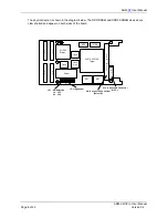
The V2PRO has 8 banks of I/O and banks 0 and 1 provide the User IO to the front panel . The VCCIO voltage
for banks 0 and 1 is selectable using JP1.
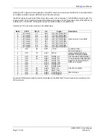
JP1 Link Posn
VCCIO – Front IO
1-2 +3V3
2-3 +2V5
5.1 Configuration
The target FPGA can be configured using two primary mechanisms. In the first, JTAG from the J6 header can
be used to perform downloading of bit-streams as well as remote debug using tools such as GDB and
ChipScope / Pro. The drawback of using JTAG is that a download cable must be connected to the board.
The XP provides a SelectMAP port between the bridge and the target device mapped to the PCI bus. This
enables very rapid download of configuration data controlled by driver and API code in the host. The maximum
speed that can be achieved is 33 Mbytes per second.
5.2 Clocks
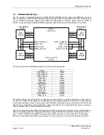
There are a number of clock sources in the XP as shown in the diagram below. Although the ICS307 is shown
connected to the bridge, which may appear differently from the block diagram in the previous section, the
purpose is to provide level translation between the 3.3V output of the clock generator and the 2.5V inputs of
the 2VP70.
ICS307
14.318MHz
OSC
CLKGEN_CLK1
CLKGEN_CLK2
2V1500
PCI
Bridge
2VP70
100/125
Virtex
PRO
LCLK
MCLK
OSC
125MHz
Differential
PCI 33/66 MHz
XRM
Interface
Bank1 Pair 0S/1P
Bank1 Pair 2S/3P
Bank0 Pair 4S/5P
3.3V signalling
2.5V signalling
Control
Bank0 Pair 6S/7P
The V2PRO has a dedicated clock for gigabit operation using the Epson 2121CA 125MHz device. This is input
on GCLK4S/5P in bank 5 and should be received in differential LVDS mode. Because of the routing limitations


