ADM-VPX3-9Z2 User Manual
V1.1 - 16th January 2020
3.1.1 Switch Definitions
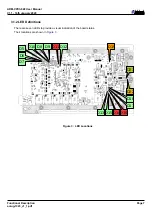
There are two push-button reset switches on the board. Their functions are detailed below.
Switch Ref.
Function
ON State
Off State
SW1
Hardware
Reset
Hardware Reset (complete restart)
Normal Operation
SW2
Software Reset Software Reset (warm reset)
Normal Operation
Table 3 : Reset Switch Definitions
There are two sets of eight DIP switches placed on the bottom of the board. Their functions are described below.
Note:
All switches are OFF by default. Factory Configuration switch must be in the OFF position for normal
operation.
Switch Ref.
Function
ON State
Off State
SW3-1
Spare (to FPGA
pin AM14)
User defined
User defined
SW3-2
Internal
Oscillator
Use VPX REFCLK
Use Internal Oscillator source
SW3-3
Internal SATA
SSD Enable
Internal SSD is connected to PS
HSSIO lane 1
PCIe lane (1) is connected to PS
HSSIO lane 1
SW3-4
Flash Boot
Inhibit
Target FPGA is not configured from
onboard flash memory.
Target FPGA is configured from on-
board flash memory.
SW3-5
VPX JTAG
Connect JTAG chain to P0
Isolate JTAG chain from P0
SW3-6
HSSIO_MUX_
SELECT A
FPGA MGT Bank 129 routed to FMC+
Socket
FPGA MGT Bank 129 connected to
V66.4 Fibre
SW3-7
Factory
Configuration
-
Normal Operation
SW3-8
HSSIO_MUX_
SELECT B
FPGA MGT Bank 130 routed to FMC+
Socket
FPGA MGT Bank 130 connected to
VPX P1
Table 4 : VPX Control Switch Definitions (SW3)
Switch Ref.
Function
ON State
Off State
SW4-(4:1)
PS_MODE(3:0) PS Boot Mode - see section
SW4-5
PS_MUX_SEL0
PS HSSIO lane 0 connected to PCIe
(0)
PS HSSIO lane 0 connected to VPX
P1
SW4-6
PS_MUX_SEL1
PS HSSIO lanes (2:1) connected to
PCIe(2:1)
PS HSSIO lanes (2:1) connected to
VPX P1
SW4-7
nSD_EMMC
SD Card enabled
eMMC device enabled
SW4-8
SD_WP
SD Card Write Protected (must be
enabled in software)
SD Card Write Enabled
Table 5 : Processor Setup Switch Definitions (SW4)
Page 6
Functional Description
ad-ug-1323_v1_1.pdf


