ADM-VPX3-9Z2 User Manual
V1.1 - 16th January 2020
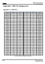
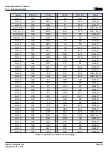
3.8.3 FMC+ GPIO Interface
The FMC+ Connector (J1) has GPIO connections arranged as follows:
Group
FPGA
Bank
Name
Function
LA_0
66
LA(12:2)
11 diff. Pairs / 22 single-ended
LA_CC (1:0)
2x Regional Clocks / GPIO pairs / 4 single-ended
LA_1
65
LA(33:19)
15 diff. Pairs / 30 single-ended
LA_CC (18:17)
2x Regional Clocks / GPIO pairs / 4 single-ended
HA_0
66,67
HA(16:2)
15 diff. Pairs / 30 single-ended
HA_CC (1:0)
2x Regional Clocks / GPIO pairs / 4 single-ended
HA(23:18)
6 diff. Pairs / 12 single-ended
HA_CC (17)
Regional Clock / GPIO pair / 2 single-ended
HB_0
64
HB(5:1)
5 diff. Pairs / 10 single-ended
HB(16:7)
10 diff. Pairs / 20 single-ended
HB(21:18)
4 diff. Pairs / 8 single-ended
HB_CC (0)
Regional Clock / GPIO pair / 2 single-ended
HB_CC (6)
Regional Clock / GPIO pair / 2 single-ended
HB_CC (17)
Regional Clock / GPIO pair / 2 single-ended
Table 22 : FMC+ Groups (J1)
3.8.4 VPX P2 GPIO Interface
The P2 VPX Connector has GPIO connections arranged as follows:
Group
FPGA
Bank
Name
Function
GPIO_0
48
GP(8:1)
8 diff. Pairs / 16 single-ended
GPIO_1
47
GP(12:9)
4 diff. Pairs / 8 single-ended
Table 23 : VPX P2 GPIO Groups
3.9 System Monitoring
The 9Z2 has the ability to monitor temperature and voltage to maintain a check on the operation of the board.
The monitoring is implemented using an Atmel AVR microcontroller (uC).
The microcontroller continually measures all voltage rails and temperature sensors and transmits the results to
the FPGA, where they are stored in blockram.
The following voltage rails and temperatures are monitored by the microcontroller:
Page 17
Functional Description
ad-ug-1323_v1_1.pdf


