5
GR-UT699 Development Board
User Manual
LIST OF FIGURES
Figure 1-1: GR-UT699 Development Board.....................................................................................8
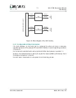
Figure 2-1: Block Diagram of GR-UT699 board.............................................................................11
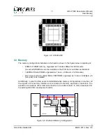
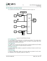
Figure 2-2: UT699 ASIC.................................................................................................................12
Figure 2-3: On-Board Memory Configuration.................................................................................13
Figure 2-4: Block Diagram of the CAN interface............................................................................14
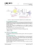
Figure 2-5: Transceiver and Termination Configuration (one of 2 interfaces shown).....................15
Figure 2-6: Transceiver and Termination of the SPW interfaces (2 of 4 interfaces shown)............16
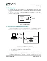
Figure 2-7: Serial interface.............................................................................................................17
Figure 2-8: Debug Support Unit connections.................................................................................17
Figure 2-9: Clock Distribution Scheme...........................................................................................19
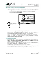
Figure 2-10: Power Regulation Configuration.................................................................................20
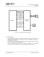
Figure 2-11: Block diagram of Ethernet Interface...........................................................................21
Figure 2-12: Block diagram for PCI System Slot connections........................................................22
Figure 2-13: Block diagram of PCI Peripheral connections............................................................23
Figure 2-14: PIO interface..............................................................................................................24
Figure 2-15: Watchdog configuration.............................................................................................25
Figure 2-16: Mezzanine Connector Pin Number Ordering..............................................................26
Figure 3-1: GRMON Output Screenshot #1...................................................................................29
Figure 3-2: GRMON Output Screenshot #2...................................................................................31
Figure 4-1: Front Panel View (pin 1 of connectors marked)...........................................................33
Figure 4-2: PCB Top View..............................................................................................................44
Figure 4-3: GR-UT699 Assembly Photo.........................................................................................45
REVISION HISTORY
Revision
Date
Page
Description
0.1 DRAFT
2008-05-01 All
New document/draft
0.2
2008-09-16 §2.5.2
§2.12.1
18
41
Added note about SPWCLK oscillator
Added notes about PCI_INT[A B C D] signals
Modified Figure 2-9
Updated Figure 4-2.
0.3
2008-10-27 All
Formatting changes
0.4
2009-01-07 7,28,29,
41,42
Updated Figure 1-1, Figure 3-1, Figure 3-2, Figure 4-2, Figure 4-3
0.5
2012-12-10 §1.2
§2.3.4
§2.12.15
Added a link to reference document about Mezzanine Connectors
Added description of Mezzanine connectors and pin numbering
0.6
2013-03-28 §2.11.1,
§2.11.2
§3
Corrected references to JP8 / JP10 in PCI jumper configurations
Added paragraph explaining grmon command for using Digilent HS-1 JTAG
cable.
© Aeroflex Gaisler AB
March 2013, Rev. 0.6
Содержание GR-UT699
Страница 1: ...GR UT699 Development Board User Manual AEROFLEX GAISLER AB Rev 0 6 2013 03 28 ...
Страница 6: ...6 GR UT699 Development Board User Manual Intentionally Blank Aeroflex Gaisler AB March 2013 Rev 0 6 ...
Страница 41: ...41 GR UT699 Development Board User Manual Aeroflex Gaisler AB March 2013 Rev 0 6 Figure 4 2 PCB Top View ...


