background image

39

GR-UT699 Development Board

User Manual

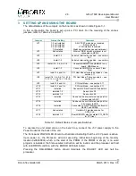
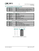
4.2  List of Oscillators, Switches and LED's

Name

Function

Description

X1

OSC_MAIN

Main oscillator for ASIC DIL8 socket, 3.3V (75MHz as standard)

X2

OSC_ETH

Oscillator for Ethernet PHY transceiver, SMD type, 3.3V, 25.000MHz

X3

OSC_SPW

DIL8 socket for user installed SPW Clock Oscillator, 3.3V

Table 4-18: List and definition of  Oscillators

Name

Function

Description

D1

POWER (3.3V)

Power indicator

D2

ERRORN

Leon processor in 'ERROR' mode

D3

DSUACT

Leon Debug Support Unit 'Active'

D4

WDOG

Watchdog indicator

D5

PROM_BUSY

Prom Write/Erase in Progress

D12

DSU_ACTIVITY

Bi-color LED indicating RX and TX activity on Serial DSU (USB) interface

Table 4-19: List and definition of PCB mounted LED's

Name

Function

Description

S1

RESET

Push button RESET switch

S2

DSU_BREAK

Push button DSU_BREAK  switch

S3

PIO[7..0]

8 pole dip switch for PIO configuration – see Table 4-21

S4

PIO[15..8]

8 pole dip switch for PIO configuration – see Table 4-22

Table 4-20: List and definition of Switches

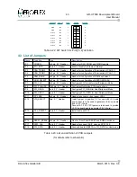
FUNCTION

ASIC pin

OPEN

SWITCH

CLOSED

PIO0

191

'1'

1

'0'

PIO1

192

'1'

2

'0'

PIO2

193

'1'

3

'0'

PIO3

194

'1'

4

'0'

PIO4

196

'1'

5

'0'

PIO5

197

'1'

6

'0'

PIO6

198

'1'

7

'0'

PIO7

199

'1'

8

'0'

Table 4-21: DIP Switch S3 'PIO[7..0]' definition

© Aeroflex Gaisler AB

March 2013, Rev. 0.6

Содержание GR-UT699

Страница 1: ...GR UT699 Development Board User Manual AEROFLEX GAISLER AB Rev 0 6 2013 03 28 ...

Страница 2: ...ich may result from its use No license is granted by implication or otherwise under any patent or patent rights of Aeroflex Gaisler AB Aeroflex Gaisler AB tel 46 31 7758650 Kungsgatan 12 fax 46 31 421407 411 19 Göteborg sales gaisler com Sweden www aeroflex com gaisler Copyright 2013 Aeroflex Gaisler All information is provided as is There is no warranty that it is correct or suitable for any purp...

Страница 3: ...upport Unit DSU Serial Interface 17 2 8 Oscillators and Clock Inputs 19 2 8 1 System Clock 19 2 8 2 SPW_CLK 19 2 8 3 Ethernet Clock 19 2 8 4 PCI Clock 20 2 9 Power Supply and Voltage Regulation 20 2 10 Ethernet Interface 20 2 11 PCI Interface 21 2 11 1 Host System Slot Configuration 22 2 11 2 Peripheral Slot Configuration 23 2 12 Other Interfaces and Circuits 24 2 12 1 GPIO 24 2 12 2 Reset Circuit...

Страница 4: ...J8 SPW 3 interface connections 36 Table 4 11 Expansion connector J9 Pin out see section 2 12 5 for pin order 38 Table 4 12 J10 PIO Header Pin out 38 Table 4 13 Expansion connector J11 Pin out see section 2 12 5 for pin order 39 Table 4 14 J12 DSU Serial over USB MiniAB 40 Table 4 15 J13 POWER External Power Connector 40 Table 4 16 J14 POWER External Power Connector 40 Table 4 17 SODIMM socket J15 ...

Страница 5: ...og configuration 25 Figure 2 16 Mezzanine Connector Pin Number Ordering 26 Figure 3 1 GRMON Output Screenshot 1 29 Figure 3 2 GRMON Output Screenshot 2 31 Figure 4 1 Front Panel View pin 1 of connectors marked 33 Figure 4 2 PCB Top View 44 Figure 4 3 GR UT699 Assembly Photo 45 REVISION HISTORY Revision Date Page Description 0 1 DRAFT 2008 05 01 All New document draft 0 2 2008 09 16 2 5 2 2 12 1 18...

Страница 6: ...6 GR UT699 Development Board User Manual Intentionally Blank Aeroflex Gaisler AB March 2013 Rev 0 6 ...

Страница 7: ...PARCTM V8 Processor ASIC device The UT699 is a Leon3FT based custom ASIC for Aerospace applications The GR UT699 Unit comprises a custom designed PCB with a 6U Compact PCI front panel making the board suitable either for stand alone bench top development or for installation in a 6U High Compact PCI rack All the principle interfaces and functions are accessible on front panel connectors The interfa...

Страница 8: ...nt UT699RH ASIC Memory SRAM 80 Mbit 1 banks x 2Mword x 40 bit typ 10ns optional second bank is not fitted as standard SDRAM SODIMM socket up to 64Mword x 40 bit with 512Mbyte module FLASH 128Mbit 4M x 32 bit typ 90ns EEPROM DIL32 socket 1 bank x 1Mbit organised x8 bit wide additional memory via memory expansion connector Interfaces two CAN interfaces four Spacewire LVDS electrical interfaces one s...

Страница 9: ...not in use store the unit in an electrostatic protective container or bag When configuring the jumpers on the board or connecting disconnecting cables ensure that the unit is in an unpowered state 1 4 Abbreviations DIL Dual In Line ESD Electro Static Discharge FP Front Panel FT Fault Tolerant GPIO General Purpose Input Output I O Input Output IP Intellectual Property LVDS Low Voltage Digital Signa...

Страница 10: ...upply The board is fitted with a Compact PCI front panel and is compatible with mounting in a 6U Compact PCI rack 2 2 UT699 ASIC The UT699RH ASCI is packaged in a 352 pin Ceramic Quad Flatpack and is soldered in to the PCB Details of the interfaces operation and programming of the UT699 ASIC is given in the UT699 Datasheet RD 3 Aeroflex Gaisler AB March 2013 Rev 0 6 UT699RH ASIC SPW ETHER NET PHY ...

Страница 11: ...its wide to be installed Additionally in order to allow users to install alternative memory configurations or devices all the signals of the memory interface are connected to memory expansion connectors The expansion connectors allow mezzanine boards to be added similar to those developed for the existing GR CPCI development boards Aeroflex Gaisler AB March 2013 Rev 0 6 Figure 2 2 UT699 ASIC Figur...

Страница 12: ...2 0 settings refer to the Memory Configuration documentation in the Leon3 User Manual or RD 3 2 3 3 EEPROM The GR UT699 board additionally has a DIP32 socket suitable for mounting an EEPROM device The data bus width to the EEPROM device is 8 bits wide This socket is suitable for mounting an EEPROM device of the type AT28LV010 or compatible in DIP32 package The AT28LV010 is an ATMEL EEPROM of 1Mbit...

Страница 13: ... with a nominal 120 Ohm insert jumpers in position 1 3 However if a split termination is desired if required for improved EMC performance insert the jumpers in positions 1 2 and 3 4 For stub nodes if termination is not required do not install any jumpers Aeroflex Gaisler AB March 2013 Rev 0 6 Figure 2 4 Block Diagram of the CAN interface CAN TRANSCEIVER CAN TRANSCEIVER CAN_H CAN_L TXD RXD CAN inte...

Страница 14: ... the following slew rates 10kOhm 15V us 100kOhm 2V us 2 5 Spacewire LVDS Interfaces The UT699 ASIC provides four Spacewire interfaces which are routed to the front panel of the board 2 5 1 SPW interface circuit Each Spacewire interface consists of 4 LVDS differential pairs 2 input pairs and 2 output pairs as shown in the figure below As the Spacewire interface to the UT699 ASIC is LVTTL 3 3V logic...

Страница 15: ... SPWCLK oscillator if appropriate Oscillator X3 is mounted in socket and jumper J17 is not installed Main processor oscillator X1 if jumper J17 is installed External clock input via SMA connector J16 X3 and J17 not installed The default configuration is that the clock is supplied by the SPWCLK oscillator X3 and jumper J17 is not installed Do not install jumper J17 if an oscillator is installed in ...

Страница 16: ...e UT699 ASIC as represented in Figure 2 8 The board provides two possibilities for connecting to the processor s DSU interface 1 USB MiniAB connector with USB to Serial interface chip 2 JTAG DSU interface The baud rate of the serial link is specified by the host computer and the DSU interface in the UT699 ASIC auto detects and adjusts its baud rate to suit The DSUENable signal input to the process...

Страница 17: ... PCB to indicate the conditions of the DSUACT signal from the UT699 processor Additionally connections are provided to an LED indicator on the front panel of the Unit A miniature push button switch is provided on the Main PCB for the DSUBREAK control and connections are provided to an additional push button switch on the front panel of the unit Aeroflex Gaisler AB March 2013 Rev 0 6 ...

Страница 18: ... 2 8 3 Ethernet Clock A dedicated 25MHz SMD oscillator is provided for the Ethernet Controller and PHY circuit see section 2 10 2 8 4 PCI Clock A dedicated 33 3MHz SMD oscillator and zero delay buffer are provided for the PCI clock For information on the configuration please see section 2 11 Aeroflex Gaisler AB March 2013 Rev 0 6 Figure 2 9 Clock Distribution Scheme SPW CLK SMD ZERO DELAY BUFFER Z...

Страница 19: ...H ASIC device incorporates a Ethernet controller with support for MII interface and the GR UT699 Development Board has an Intel LXT971 10 100Mbit s Ethernet PHY transceiver and RJ45 connector are on board For more information on the registers and functionality of the Ethernet MAC PHY device please refer to the data sheet for the WJLXT971A device A 25MHz oscillator dedicated for this device is prov...

Страница 20: ... either as a peripheral slot card or system slot card as described in the following sections Note that the GR UT699 board has been designed to operate in a 3 3V signalling environment and the Compact PCI connector is appropriately keyed yellow key Aeroflex Gaisler AB March 2013 Rev 0 6 Figure 2 11 Block diagram of Ethernet Interface UT699RH ETH_RXCLK 25MHz ETHERNET PHY ETH_TXCLK RJ45 ETH_RXD 3 0 4...

Страница 21: ...the card operating in the system slot PCI_FRAMEN PCI_IRDYN PCI_TRDYN PCI_DEVSELN PCI_STOPN PCI_PERRN PCI_SERRN PCI_LOCKN This can be achieved by installing the JP8 jumpers 1 2 3 4 5 6 7 8 9 10 11 12 13 14 15 16 17 18 and 19 20 In order to ensure that the PCIRSTN pin on the back plane is not left floating it is also Aeroflex Gaisler AB March 2013 Rev 0 6 ASIC BUFFER XTAL 33MHz JP7 PCICLK1 PCICLK2 P...

Страница 22: ...the backplane and connects its REQN GNTN signals to the backplane REQN GNTN signals Figure 2 13 Block diagram of PCI Peripheral connections This requires the jumpers to be installed as follows JP7 1 3 JP9 2 3 JP10 2 3 The jumpers in JP8 and JP18 should be not be installed Aeroflex Gaisler AB March 2013 Rev 0 6 ASIC BUFFER XTAL 33MHz JP7 PCICLK1 PCICLK2 PCICLK PCICLKIN REQ IDSEL GNTN IDSEL GNT ARBI...

Страница 23: ...ve PCI interrupts from the backplane if desired If the board is installed in a CPCI rack setting resetting the GPIO 11 8 may therefore cause unintended behaviour by generating a generating PCI Interrupts on the back plane If this behaviour is not desired disconnect the GPIO signals from the PCI interrupts on the back plane by removing resistor pack R35 2 12 2 Reset Circuit and Button A standard Pr...

Страница 24: ...will illuminate but a system reset will not occur 2 12 4 JTAG interface A 14 pin connector on the front panel provides the possibility to connect to the JTAG signals and JTAG chain of the UT699 ASIC This interface allows DSU Debug over the JTAG interface to be performed 2 12 5 Mezzanine Memory Expansion Two connectors J9 and J11 are provided on the board which give access to the memory bus signals...

Страница 25: ...in the Technical Note RD 4 Therefore please take care when designing your own mezzanine boards to take account of this pin ordering If there is any confusion or you have any doubts please do not hesitate to contact info pender ch Additional dimensional data or Gerber layout information can be provided if required to aid in the layout of the User s mezzanine board Aeroflex Gaisler AB March 2013 Rev...

Страница 26: ...see section 2 11 JP10 Install 1 2 and 3 4 PCI Host Mode see section 2 11 JP11 Installed Connects to Front Panel LED indicators JP12 Installed 1 2 See section 2 9 JP13 Installed 1 2 See section 2 9 JP14 Installed Can be used as current measure point for Vcore supply to ASIC JP15 Installed Can be used as current measure point for 3 3V supply to ASIC JP16 Installed Connected to Front Panel push butto...

Страница 27: ...iated hardware dongle Starting GRMON with the command grmon i will establish a link to the DSU and will initialise the processor registers and timers The default serial interface used by GRMON is dev ttyS0 linux or com1 Windows To use a different serial interface specify the command grmon i uart dev comXX where XX is the number of the com port In the example shown in Figure 3 1 a connection is bei...

Страница 28: ...28 GR UT699 Development Board User Manual Aeroflex Gaisler AB March 2013 Rev 0 6 Figure 3 1 GRMON Output Screenshot 1 ...

Страница 29: ...29 GR UT699 Development Board User Manual Aeroflex Gaisler AB March 2013 Rev 0 6 Figure 3 2 GRMON Output Screenshot 2 ...

Страница 30: ...ewire Interface 2 J8 SPW 3 MDM9 S female LVDS connections for Spacewire Interface 3 J9 MEM I O AMP 5177984 5 Memory I O connector 120 pin 0 8mm pitch J10 GPIO 15 0 34 pin 0 1 Header Pin connections for PIO signals 0 to 15 J11 GEN I O AMP 5177984 2 General I O connector 80 pin 0 8mm pitch J12 DSU SERIAL USB MINI AB Debug Support Unit serial I F via on board USB converter J13 POWER IN 2 1mm center v...

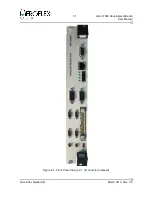
Страница 31: ...31 GR UT699 Development Board User Manual Figure 4 1 Front Panel View pin 1 of connectors marked Aeroflex Gaisler AB March 2013 Rev 0 6 ...

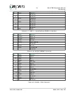
Страница 32: ... Output ve 2 TPFON Output ve 3 TPFIP Input ve 4 TPFOC Output centre tap 5 No connect 6 TPFIN Input ve 7 TPFIC Input centre tap 8 No connect Table 4 3 J2 RJ45 ETHERNET Connector Pin Name Comment 1 DGND Ground 2 VREF 3 3V 3 DGND Ground 4 TMS JTAG TMS 5 DGND Ground 6 TCK JTAG TCK 7 DGND Ground 8 TDO JTAG TDO 9 DGND Ground 10 TDI JTAG TDI 11 DGND Ground 12 NC No connect 13 DGND Ground 14 NC No connect...

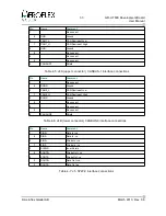
Страница 33: ... No connect 6 DGND Ground 2 CAN0_L CAN Dominant Low 7 CAN0_H CAN Dominant High 3 DGND Ground 8 No connect 4 No connect 9 No connect 5 CANSHD0 Shield Table 4 6 J4B lower connector CANBUS 0 interface connections Pin Name Comment 1 DIN0 Data In ve 6 DIN0 Data In ve 2 SIN0 Strobe In ve 7 SIN0 Strobe In ve 3 SHIELD Inner Shield 8 SOUT0 Strobe Out ve 4 SOUT0 Strobe Out ve 9 DOUT0 Data Out ve 5 DOUT0 Dat...

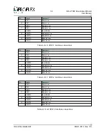
Страница 34: ... DIN2 Data In ve 6 DIN2 Data In ve 2 SIN2 Strobe In ve 7 SIN2 Strobe In ve 3 SHIELD Inner Shield 8 SOUT2 Strobe Out ve 4 SOUT2 Strobe Out ve 9 DOUT2 Data Out ve 5 DOUT2 Data Out ve Table 4 9 J7 SPW 2 interface connections Pin Name Comment 1 DIN3 Data In ve 6 DIN3 Data In ve 2 SIN3 Strobe In ve 7 SIN3 Strobe In ve 3 SHIELD Inner Shield 8 SOUT3 Strobe Out ve 4 SOUT3 Strobe Out ve 9 DOUT3 Data Out ve...

Страница 35: ...39 A27 A24 33 29 92 34 A25 3 3V 30 91 3 3V DGND 31 90 DGND A22 31 32 89 32 A23 A20 28 33 88 29 A21 A18 26 34 87 27 A19 A16 23 35 86 24 A17 A14 21 36 85 22 A15 A12 18 37 84 19 A13 A10 16 38 83 17 A11 A8 11 39 82 12 A9 3 3V 40 81 3 3V DGND 41 80 DGND A6 9 42 79 10 A7 A4 6 43 78 7 A5 A2 4 44 77 5 A3 A0 1 45 76 2 A1 WRITEN 98 46 75 139 READ OEN 99 47 74 102 IOSN ROMSN0 103 48 73 104 ROMSN1 RAMSN4 123 ...

Страница 36: ...1 29 30 DGND GPIO15 262 31 32 DGND 3 3V 33 34 DGND Table 4 12 J10 PIO Header Pin out FUNCTION ASIC pin CONNECTOR PIN FUNCTION DGND 1 60 DGND CB6 96 2 59 97 CB7 CB4 93 3 58 94 CB5 CB2 91 4 57 92 CB3 CB0 89 5 56 90 CB1 6 55 7 54 8 53 9 52 DGND 10 51 DGND 3 3V 11 50 3 3V 12 49 13 48 14 47 15 46 16 45 17 44 18 43 19 42 DGND 20 41 DGND 3 3V 21 40 3 3V 22 39 23 38 PCIIO6 24 37 PCIIO7 PCIIO4 25 36 PCIIO5...

Страница 37: ...und Table 4 14 J12 DSU Serial over USB MiniAB Pin Name Comment VE 5V Inner Pin 5V typically TBD A VE GND Outer Pin Return Table 4 15 J13 POWER External Power Connector Pin Name Comment 1 5V 5V typically TBD A 2 GND Ground 3 12V 12V Not used 4 GND Ground Table 4 16 J14 POWER External Power Connector Aeroflex Gaisler AB March 2013 Rev 0 6 ...

Страница 38: ...SDRASN 65 66 SDCASN SDWEN 67 68 SDCKE1 pulled high SDCSN0 69 70 A17 SDCSN1 71 72 A14 nc 73 74 SDCLK1 DGND 75 76 DGND nc 77 78 nc nc 79 80 nc 3 3V 81 82 3 3V D15 83 84 nc D14 85 86 nc D13 87 88 nc D12 89 90 nc DGND 91 92 DGND D11 93 94 nc D10 95 96 nc D9 97 98 nc D8 99 100 nc 3 3V 101 102 3 3V A8 103 104 A9 A10 105 106 A15 SBA0 DGND 107 108 DGND A11 109 110 A16 SBA1 A12 111 112 A13 3 3V 113 114 3 3...

Страница 39: ...Watchdog indicator D5 PROM_BUSY Prom Write Erase in Progress D12 DSU_ACTIVITY Bi color LED indicating RX and TX activity on Serial DSU USB interface Table 4 19 List and definition of PCB mounted LED s Name Function Description S1 RESET Push button RESET switch S2 DSU_BREAK Push button DSU_BREAK switch S3 PIO 7 0 8 pole dip switch for PIO configuration see Table 4 21 S4 PIO 15 8 8 pole dip switch f...

Страница 40: ...figures PCI Clocks for Host Peripheral Mode JP8 PCI_PULLUPS 10x2 pin 0 1 Header Configures Host mode PCI signal pull ups JP9 PCI_REQN 4 pin 0 1 Header Configures PCI_REQN for Host Peripheral Mode JP10 PCI_GNTN 4 pin 0 1 Header Configures PCI_GNTN for Host Peripheral Mode JP11 FP_LEDS 4x2 pin 0 1 Header Header to connect or front panel LED s JP12 VIN_SELECT 3pin 0 1 Header Install jumper in positio...

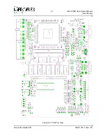
Страница 41: ...41 GR UT699 Development Board User Manual Aeroflex Gaisler AB March 2013 Rev 0 6 Figure 4 2 PCB Top View ...

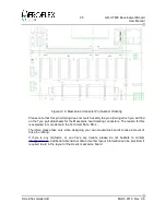
Страница 42: ...42 GR UT699 Development Board User Manual Aeroflex Gaisler AB March 2013 Rev 0 6 Figure 4 3 GR UT699 Assembly Photo ...

Отзывы: