background image


IP482 Industrial I/O Pack User’s Manual                                Counter Timer Module 

__________________________________________________________________ 

_________________________________________________________________________________________  

  Acromag, Inc.  Tel:248-295-0310  Fax:248-624-9234  Email:[email protected] http://www.acromag.com 

32 


Input Period Measurement 


The counter/timer may be used to measure the period of an input signal 

at the counter input InA.  Setting bits 2 to 0 of the Counter Control Register 
to logic “110” configures the counter for period measurement.  The first input 
cycle after period measurement is triggered will be measured. 

 
InA is used to input the signal to be measured.  Period measurement can 

be initiated on the active low or high portion of the waveform.  The period of 
signal is the time the signal is low added to the time the signal is high, 
before it repeats. 

 
InB can be used to input an external clock for period measurement.  Bits 

7 and 6 must be set to either logic “01” or “10”.  Additionally, the clock 
source bits 12, 11, and 10 must be set to logic “101” to enable external clock 
input.  Period measurement can alternatively be internally clocked using 
control register bits 12, 11, and 10.  Available frequencies vary depending 
on carrier operational frequency.   

 
InC can be used to externally trigger period measurement.  Additionally, 

Period Measurement can be triggered internally via the Counter Trigger 
Register at the base a offset 04H.  An initial trigger, software or 
external, starts period measurement at the beginning of the next active 
period. 
 

The period being measured serves as an enable control for an up-

counter whose value can be read from the Counter Read Back Register.  
When triggered the counter is reset.  Then, the active polarity of InA starts 
period measurement.  The counter increments by one for each clock pulse 
during the input signal period (InA).  The resultant period is equivalent to the 
count value read from the Counter Read Back Register, multiplied by the 
clock period.  A 1.75

s output pulse will be generated at the counter output 

pin to signal the completion of a given measurement.  Note that the 
measured period may be in error by 

 1 clock cycle. 

 
Reading a counter value of 0xFFFF hex indicates that the pulse duration 

is longer than the current counter size and clock frequency can measure.  
Upon reading of this overflow value you must select a slower frequency and 
re-measure. 

 
An interrupt can be generated upon completion of a given period 

measurement, if enabled via the interrupt enable bit of the Counter Control 
Register (bit 15).  The interrupt will be generated upon completion of the first 
complete waveform cycle after the counter is triggered.  The interrupt will 
occur even if an external clock is selected but no clock signal is provided on 
InB.  The count value will be zero in this case.  The interrupt, once driven 
active, will remain pending until released by setting the required bit of the 
Interrupt Status/Clear


register at the base a offset 02H.  A pending 

interrupt can also be cleared, by setting Counter Control register bit-15 to 
logic low. 

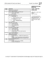
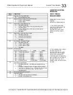
COUNTER CONTROL 
REGISTER 

Содержание IP482 Series

Страница 1: ...USER S MANUAL ACROMAG INCORPORATED Tel 248 295 0310 30765 South Wixom Road Fax 248 624 9234 P O BOX 437 Wixom MI 48393 7037 U S A Copyright 2004 Acromag Inc Printed in the USA Data and specifications...

Страница 2: ...Field I O Connector P2 8 IP Logic Interface Connector P1 9 I O Noise and Grounding Considerations 10 3 0 PROGRAMMING INFORMATION IP IDENTIFICATION SPACE 11 MEMORY MAP 12 Board Control Register 14 Inte...

Страница 3: ...easurement Example 44 One Shot Pulse Mode Example 45 4 0 THEORY OF OPERATION LOGIC POWER INTERFACE 48 FIELD INPUT OUTPUT SIGNALS 48 Counter Timers 48 Digital I O 48 5 0 SERVICE AND REPAIR SERVICE AND...

Страница 4: ...motion The sequence of logic high pulses for two input signals A and B indicate direction and a third signal index is used to initialize the counter X1 X2 and X4 decoding is also implemented X1 decod...

Страница 5: ...ndard IP module footprint Up to four units may be mounted on a 6U VMEbus carrier board or five units may be mounted on a PCI carrier board Local ID Each IP module has its own 8 bit ID information whic...

Страница 6: ...to AVME9630 9660 boards within the card cage via flat 50 pin ribbon cable Model 5025 550 X or 5025 551 X Acromag provides a software product sold separately consisting of IP module ActiveX OLE control...

Страница 7: ...his board is physically protected with packing material and electrically protected with an anti static bag during shipment However it is recommended that the board be visually inspected for evidence o...

Страница 8: ...incorrect assembly P2 pin assignments are unique to each IP model see Table 2 1 and normally correspond to the pin numbers of the field I O interface connector on the carrier board you should verify...

Страница 9: ...rsh environments see Drawing 4501 434 for assembly details Field and logic side connectors are keyed to avoid incorrect assembly The pin assignments of P1 are standard for all IP modules according to...

Страница 10: ...ld I O connections are not isolated from the carrier board and backplane Two ounce copper ground plane foil has been employed in the design of this model to help minimize the effects of ground bounce...

Страница 11: ...ny variable e g unique calibration information ID space bytes are addressed using only the odd addresses in a 64 byte block on the Big Endian VMEbus Even addresses are used on the Little Endian PC ISA...

Страница 12: ...addresses shown to properly access the IP482 registers Accesses are generally performed on a 16 bit basis D0 D15 but 8 bit D0 D8 EO accesses are possible in most cases EVEN Base Addr EVEN Byte D15 D08...

Страница 13: ...stant A Register 39 3A Counter 6 Constant A Register 3B 3C Counter 7 Constant A Register 3D 3E Counter 8 Constant A Register 3F 40 Counter 9 Constant A Register 41 42 Counter 10 Constant A Register 43...

Страница 14: ...er can be read or written with either 8 bit or 16 bit data transfers A power up or system reset sets board control register bit 0 to logic 0 BIT FUNCTION 0 IP Carrier Clock Speed Read Write Bit 0 8MHz...

Страница 15: ...ll be generated again if the condition which caused the interrupt to occur remains Writing 0 to a bit location has no effect That is a pending interrupt will remain pending Writing to this register is...

Страница 16: ...2 Stop 1 2 Counter 3 Stop 1 3 Counter 4 Stop 1 4 Counter 5 Stop 1 5 Counter 6 Stop 1 6 Counter 7 Stop 1 7 Counter 8 Stop 1 8 Counter 9 Stop 1 9 Counter 10 Stop 1 10 15 Not Used 1 Writing to this regis...

Страница 17: ...entifies the position of the available input bits BIT FUNCTION 0 DIn1 1 1 DIn2 1 2 7 Not Used 2 Reading this register is possible via 16 bit or 8 bit data transfers Digital Output Register Read Write...

Страница 18: ...ess to the Interrupt Status register Issue of a software or hardware reset will clear the contents of this register to 0 Counter Control Register Read Write This register is used to configure counter...

Страница 19: ...crements when B leads A For X4 encoding four increments or decrements on each edge of channel A and B result from each cycle The counter increments when A leads B and decrements when B leads A Quadrat...

Страница 20: ...Output Polarity Output Pin ACTIVE Level 0 Active LOW Default 1 1 Active HIGH 5 4 InA Channel A 00 Disabled Default 01 X1 Encoding 10 X2 Encoding 11 X4 Encoding 6 InB Channel B 0 Disabled Default 1 En...

Страница 21: ...ntrol the operation of the counter output signal With bits 11 and 10 set to 01 the output signal will be driven active while the counter equals the counter Constant A value With bit 11 set to logic 1...

Страница 22: ...maximum internal clock frequency is selected 8MHz or 32MHz a delay of one extra clock cycle will be added to the counter constant value InA can be used as a Gate Off signal to stop and start the count...

Страница 23: ...Clock Enabled 10 External Clock Enabled 11 Disabled 9 8 InC Polarity External Trigger 00 Disabled Default 01 Active LOW External Trigger 10 Active HIGH External Trigger 11 Disabled 12 11 10 Clock Sou...

Страница 24: ...101 to enable external clock input The timer can alternatively be internally clocked using control register bits 12 11 and 10 Available frequencies vary depending on carrier opertional frequency InC c...

Страница 25: ...e HIGH Trigger 11 Gate Off Continue when high Stop when low 12 11 10 Clock Source 2 Carrier Operational Freq 8MHz 32MHz 000 Internal Default 0 5MHz 2MHz 001 Internal 1MHz 4MHz 010 Internal 2MHz 8MHz 0...

Страница 26: ...egister bits 7 and 6 A minimum event pulse width InB of 125ns is required for correct pulse detection with input debounce disabled Programmable clock selection is not available in event counter mode I...

Страница 27: ...InB Polarity Event Input 00 Disabled Default 01 Active LOW Events 10 Active HIGH Events 11 Disabled 9 8 InC Polarity External Trigger 00 Disabled Default 01 Active LOW Trigger 10 Active HIGH Trigger...

Страница 28: ...utput will generate a 1 75 s output pulse and an optional interrupt InC can be used as an external trigger input When control register bits 9 and 8 are set to logic 01 or 10 the InC input functions as...

Страница 29: ...Counted 00 Disabled Default 01 Active LOW Pulse Counted 10 Active HIGH Pulse Counted 11 Disabled 9 8 InC Polarity External Trigger 00 Disabled Default 01 Active LOW Trigger 10 Active HIGH Trigger 11 D...

Страница 30: ...nal starts pulse width measurement at the beginning of the next active pulse For pulse width measurement the pulse width being measured serves as an enable control for an up counter whose value can be...

Страница 31: ...ational Freq 8MHz 32MHz 000 Internal Default 0 5MHz 2MHz 001 Internal 1MHz 4MHz 010 Internal 2MHz 8MHz 011 Internal 4MHz 16MHz 100 Internal 8MHz 32MHz 101 External Clock Up to 2MHz Up to 8MHz 13 Input...

Страница 32: ...trigger software or external starts period measurement at the beginning of the next active period The period being measured serves as an enable control for an up counter whose value can be read from...

Страница 33: ...12 11 10 Clock Source Carrier Operational Freq 8MHz 32MHz 000 Internal Default 0 5MHz 2MHz 001 Internal 1MHz 4MHz 010 Internal 2MHz 8MHz 011 Internal 4MHz 16MHz 100 Internal 8MHz 32MHz 101 External Cl...

Страница 34: ...start the counter and thus output When InA is enabled via bits 5 and 4 of the control register for active low Gate Off input a logic low input will enable the one shot counter while a logic high will...

Страница 35: ...Trigger 10 Active HIGH Trigger 11 Disabled 12 11 10 Clock Source 2 Carrier Operational Freq 8MHz 32MHz 000 Internal Default 0 5MHz 2MHz 001 Internal 1MHz 4MHz 010 Internal 2MHz 8MHz 011 Internal 4MHz...

Страница 36: ...ounter is reloaded to zero Additionally debounce is enabled 1 Connect the inputs output to the following pins unpowered Pin Connection Description 1 In1_A Channel A 11 In1_B Channel B 21 In1_C Index 3...

Страница 37: ...ing 16 bit Counter 3 The counter has an external active high gate off trigger and clock signals The output is active high Assume the external clock has a frequency of 500KHz The Gate Off signal will b...

Страница 38: ...it has been stipulated that the pulse is active high 3H is written to Counter 3 Constant A Register which contains the value for the non active low portion of the pulse The same procedure is used to c...

Страница 39: ...Enables interrupts 3 Write the 16 bit value 5H to Counter 5 Constant A Register located at the base address plus an offset of 38H In order to determine the correct Constant A Register value first calc...

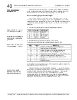
Страница 40: ...ed at base address plus an offset of 14H Bits Logic Operation 2 1 0 100 Sets the counter to Event Counting mode 3 0 Sets the output to active low 5 4 01 Enable the Gate Off input InA to active low 7 6...

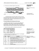
Страница 41: ...has an active low External Trigger The output of the counter is active low and interrupts and debounce are enabled Assume the enable pulse has a duration of 50 s 1 Connect the inputs output to the fol...

Страница 42: ...enable signal Therefore the frequency is 9 50 s which is equal to 180KHz Note that the counter must be re triggered before the next frequency measurement can take place Additionally the output pulse i...

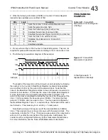
Страница 43: ...iplying the number in the Counter 9 Read Back Register located at base address plus an offset of 2CH by the period of the selected clock Note that the value in the Read Back Register is stored in Hex...

Страница 44: ...nter to Input Period Measurement 3 1 Sets the output to active high 5 4 01 Sets the Pulse input InA to active low 7 6 01 Enables the external clock input InB 9 8 10 Enables the external Trigger Input...

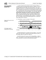
Страница 45: ...hot Pulse mode using 16 bit Counter 9 The output pulse is active high with the low portion 20 s long and the high portion 5 s long Additionally the counter has an external clock an active high Gate of...

Страница 46: ...the pulse is active high 4H is written to the Counter 9 Constant A Register which contains the value for the non active low portion of the pulse The same procedure is used to calculate the Constant B...

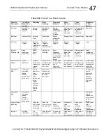
Страница 47: ...fter trigger is measured Next complete period after trigger is measured Starts Quadrature Measurement Counter Timer Output Output Waveform Output is active from trigger until terminal count 1 75 s pul...

Страница 48: ...ols for the Counter Timer modules The field I O interface to the IP module is provided through connector P2 refer to Table 2 1 These pins are tied to the inputs and outputs of EIA RS485 RS422 line tra...

Страница 49: ...been followed Also refer to the documentation of your carrier CPU board to verify that it is correctly configured Replacement of the module with one that is known to work correctly is a good technique...

Страница 50: ...Temperature Standard Unit 0 to 70 C E Version 40 to 85 C Relative Humidity 5 95 Non Condensing Storage Temperature 55 C to 125 C Non Isolated Logic and field commons have a direct electrical connecti...

Страница 51: ...titive Counter Type The IP482 has a total of ten 16 bit TTL counters available for use Each Counter has an InA InB and InC input port These TTL input ports are used to control Start Stop Reload Event...

Страница 52: ...TTL Digital Outputs 1 6 are the same as the counter inputs and outputs See the Input Electrical Characteristics and Output Electrical Characteristics sections on the previous page Specification This d...

Страница 53: ...improper installation Schematic and Physical Attributes See Drawing 4501 463 Shipping Weight 1 0 pound 0 5Kg packaged Type Termination Panel For AVME9630 9660 or APC8620 Boards Application To connect...

Страница 54: ...rcuit board depth Connects to Acromag termination panel 5025 552 from the rear of the card cage and to AVME9630 9660 boards within card cage via flat 50 pin ribbon cable cable Model 5025 551 X Schemat...

Страница 55: ...ag Inc Tel 248 295 0310 Fax 248 624 9234 Email solutions acromag com http www acromag com 55 5V 5V 4 7K P1 P2 5V OUT 1 OF 10 4 7K IN C 1 OF 10 4 7K IN A 1 OF 10 5V CLOCK COUNTER TIMER INPUT IN B 1 OF...

Страница 56: ...M C THROUGH SOLDER SIDE OF CARRIER BOARD AND INTO HEX SPACERS ITEM B AND TIGHTEN 4 PLACES THE RECOMMENDED TORQUE IS 0 226 NEWTON METER OR 2 INCH POUNDS OVER TIGHTENING MAY DAMAGE CIRCUIT BOARD 2 INSER...

Страница 57: ...le ___________________________________________________________________ ________________________________________________________________________________________ Acromag Inc Tel 248 295 0310 Fax 248 624...

Страница 58: ...le __________________________________________________________________ _________________________________________________________________________________________ Acromag Inc Tel 248 295 0310 Fax 248 624...

Страница 59: ..._________________________________________________________________ ________________________________________________________________________________________ Acromag Inc Tel 248 295 0310 Fax 248 624 9234...

Отзывы: