IP482 Industrial I/O Pack User’s Manual Counter Timer Module
__________________________________________________________________
_________________________________________________________________________________________
Acromag, Inc. Tel:248-295-0310 Fax:248-624-9234 Email:[email protected] http://www.acromag.com
14
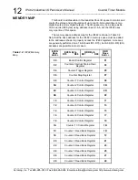
The memory map for this module is given assuming byte accesses using
the “Big Endian” byte ordering format. Big Endian is the convention used in
the Motorola 68000 and PowerPC microprocessor family and is the VMEbus
convention. In Big Endian, the lower-order byte is stored at odd-byte
addresses. The Intel x86 family of microprocessors uses the opposite
convention, or “Little Endian” byte ordering. Little Endian uses even-byte
addresses to store the low-order byte. As such, use of the memory map for
this module on a PC carrier board will require the use of the even address
locations to access the lower 8-bit data. On a VMEbus carrier use of odd
address locations are required to access the lower 8-bit data.
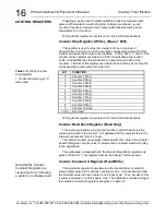
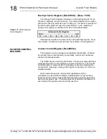
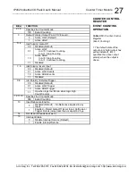
Board Control Register (Read/Write)- (Base + 00H)
This read/write register is used to identify the IP48x model, set the carrier
operational frequency, and for software reset. The function of each of the
board control register bits is described in Table 3.3. This register can be
read or written with either 8-bit or 16-bit data transfers. A power-up or
system reset sets board control register bit 0 to logic 0.
BIT
FUNCTION
0
IP Carrier Clock Speed (Read/Write Bit)
0 = 8MHz Carrier
1 = 32MHz Carrier
This bit must be set correctly for proper operation.
1 to 7
Not Used
1
10, 9, 8
Identify IP48x model. (Read Only Bits)
111 = IP482
100 = IP483
001 = IP484
11 to 14
Not Used
1
15
Software Reset: Write log
ic “1” to this bit to reset the IP482.
1
Interrupt Status/Clear Register (Read/Write)
– (Base +02H)
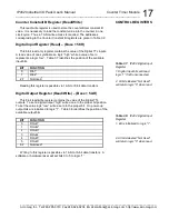
This read/write register is used to determine the pending status of the
Counter/Timer interrupts, and release pending interrupts
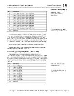
The Counter/Timer interrupt status/clear bits 0 to 9 reflect the status of
each of the Counter/Timers. A “1” bit indicates that an interrupt is pending
for the corresponding counter/timer. The Counter/Timer and its
corresponding interrupt Pending/Clear bits are as shown in Table 3.4.
Read
of this bit reflects the interrupt pending status of the counter timer
logic.
0 = Interrupt Not Pending
1 = Interrupt Pending
Write
a logic “1” to this bit to release a counter timer pending interrupt. A
counter timer pending interrupt can also be released by disabling
interrupts via bit-15 of the Counter Control registers.
MEMORY MAP
CONTROL REGISTERS
CAUTION:
Bit 0 of the
Board Control Register
must be set correctly for
proper module operation.
Table 3.3:
Board Control
Register
1. All bits labeled “Not Used”
and the Software Reset bit will
return logic “0” when read.

