Acer V551 (new) CRT Monitor Service Guide
Chapter 2 Circuit Operation Theory
21
Confidence and Property
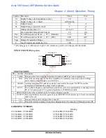
Symbol Parameter
Value
Unit
Vi
Supply Voltage (low impedance source)
30
V
Vi
Supply Voltage (li < 30mA)
self limiting
Io Ouptut
Current
±
1
A
Eo
Output Energy (capacitive load)
5
μ
J
Analog imputs( pins 2,3)
-0.3 to 55
V
Error Amplifier Output Sink Current
10
mA
Ptot
Power Dissipation at Tamb
≦
25
℃
(Minidip)
1.25 W
Ptot
Power Dissipation at Tamb
≦
25
℃
(SO8)
800 mW
Tstg
Storage Temperature Range
-65 to 150
℃
T
L
Lead Temperature (soldering 10s)
300
℃
* All voltag ges are with respect to pin 5, all currents are positive into the specified terminal.
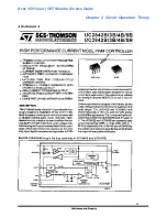
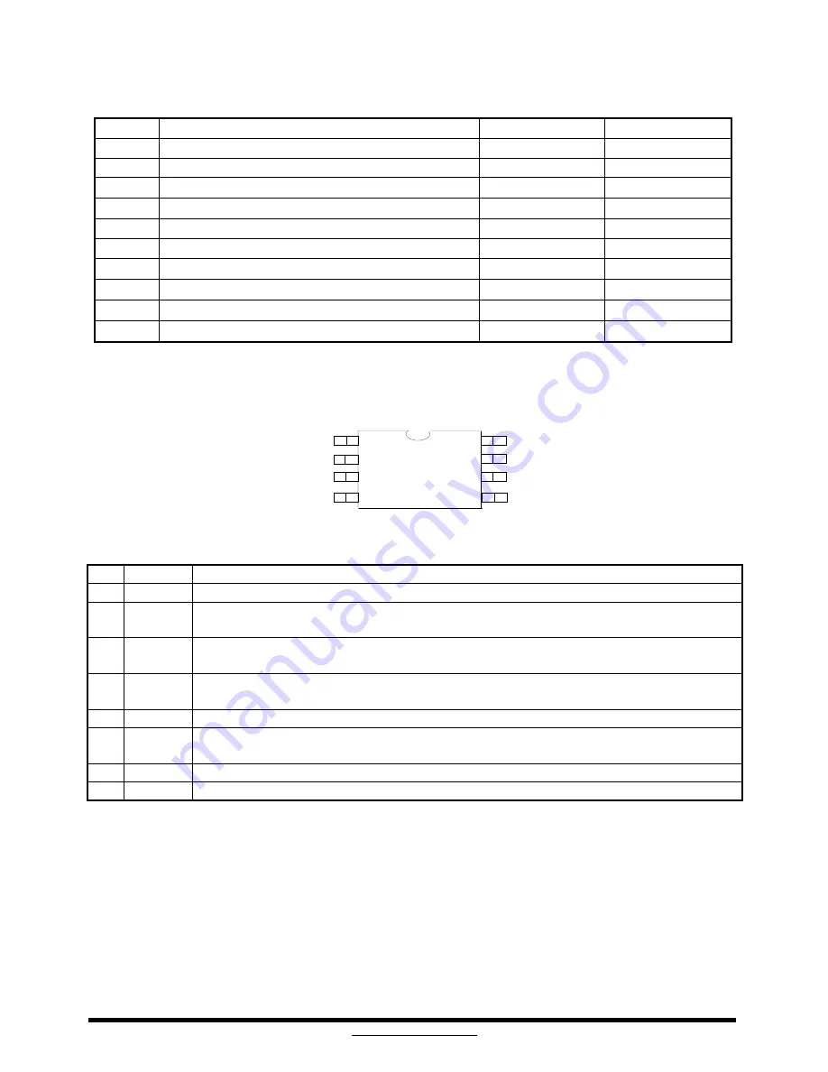
PIN CONNECTION (top view)
Minidip/SO8
COMP
V
FB
REF
V
R
T
/ C
T
i
V
SENSE
I
OUTPUT
GROUND
D95IN332
1
2
3
4
8
7
6
5
PIN FUNCTIONS
NO Function Description
1
COMP
This pin is the Error Amplifier output and is made available for loop compensation.
2
VFB
This is the inverting input of the Error Amplifier, It is normally connected to the switchingt
power supply output through a resistor divider.
3
ISENSE Avoltage proportional to inductor current is connected to this input. The PWN uses this
information to terminate the output switch conduction.
4
RT/CT
The oscillator frequency and maximum output duty cycle are programmed by connecting resistor
RT to Vref and cpacitor CT to ground. Operation to 500KHZ is possible.
5
GROUND This pin is the combined control circuitry and power ground.
6
OUTPUT This output directly drives the gate of a power MOSFET.Peak currents up to 1A are sourced and
sunk by this pin.
7
Vcc
This pin is the positive supply of the control IC.
8
Vref
This is the reference ouptput. It provides charging current for capacitor CTthrough resistor. RT.
ORDERING NUMBERS
SO8 Minidip
UC2842BD1; UC3842BD1
UC2842BN;UC3842BM
UC2843BD1; UC3842BD1
UC2843BN;UC3843BM
UC2844BD1; UC3842BD1
UC2844BN;UC3844BM
UC2845BD1; UC3842BD1
UC2845BN;UC3845BM

