


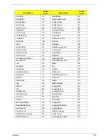


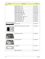


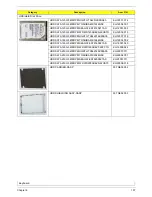


Chapter 5
145
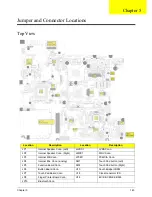
Jumper and Connector Locations
Top View
Location
Description
Location
Description
JP1
Internal Speaker Conn. (Left)
JLVDS1
LVDS Conn.
JP2
Internal Speaker Conn. (Right)
JMDC1
MDC Conn.
JP3
Internal K/B Conn.
JPCM1
PCMCIA Conn.
JP4
Internal Mic. Conn. (analog)
SW1
Touch Pad button (Left)
JP5
Function Board Conn.
SW2
Touch Pad button (Right)
JP6
Button Board Conn.
U10
South Bridge ICH9M
JP7
Touch Pad Board Conn.
U18
Clock Generator ICS
JP8
Finger Printer Board Conn.
U16
EC/ KBC ENE KB926
JP10
Bluetooth Conn.
Chapter 5
Содержание Extensa 4630G
Страница 6: ...VI...
Страница 10: ...X Table of Contents...
Страница 14: ...4 Chapter 1 System Block Diagram...
Страница 34: ...24 Chapter 1...
Страница 51: ...Chapter 2 41 3 Reboot the system and key in the selected string qjjg9vy 07yqmjd etc for the BIOS user password...
Страница 52: ...42 Chapter 2...
Страница 60: ...50 Chapter 3 7 Remove the WLAN cover as shown...
Страница 95: ...Chapter 3 85 7 Lift the Thermal Module clear of the Mainboard...
Страница 114: ...104 Chapter 3 3 Connect the RJ 11 cable to the modem module as shown...
Страница 118: ...108 Chapter 3 2 Replace the two securing screws...
Страница 122: ...112 Chapter 3 2 Connect the seven cables on the mainboard as shown B C D E F G A...
Страница 128: ...118 Chapter 3 3 Turn the computer over and replace the five securing screws...
Страница 175: ...Chapter 6 165...
Страница 184: ...Appendix A 174...
Страница 188: ...178 Appendix B...
Страница 190: ...180 Appendix C...
Страница 193: ...183 Wireless Function Failure 136 WLAN Board 52...
Страница 194: ...184...


