ACCES I/O Products, Inc.
MADE IN THE USA
mPCIe- and M.2-AIO16-16F Family Manual
7
Rev B7a
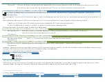
Base Clock:
Reading this 32-bit register returns the speed (in Hertz) of the clock used to generate ADC Start Conversions. Typical value is 50Million (50MHz), but for
broadest compatibility software should always read this register during init, and always use the read value when calculating what, if any, divisors to write to the
ADC Rate Divisor, DAC Waveform Rate Divisor, and Watchdog timeout registers.
ADC Rate Divisor, 10 of 32-bit Memory BAR[1]Read/Write 32-bits only
ADC Rate Divisor: Write a 32-bit divisor to the ADC Rate Divisor register to control the speed at which ADC Conversions occur in selected ADC Conversion Start Modes.
ADC Rate Divisor = integer(Base Clock ÷ Target ADC Start Rate)
Actual ADC Start Rate (Hz) = Base Clock ÷ ADC Rate Divisor
In ADC Scan Start mode each timeout of the +10 divisor begins a scan of channels. In all other modes the +10 rate selects the conversion rate per-channel.
ADC Rate Divisor #2, 14 of 64-bit Memory BAR[2+3] Read/Write 32-bits only
ADC Rate Divisor #2:
Write a 32-bit divisor to the ADC Rate Divisor #2 register to control the speed at which ADC Conversions occur within each scan when running in ADC
Scan Start Modes.
In “ADC Scan” start modes only, one Scan of ADC CH0 through the channel selec
ted in +38 INx2:0 bits occurs at the rate selected at +10. During each Scan the first channel is
converted immediately, and subsequent channels are acquired at the rate selected at +14.
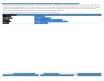
ADC Advanced Sequencer Gain Control, 18 of 32-bit Memory BAR[1]Read/Write 32-bits only
bit D31 D30 D29 D28 D27 D26 D25 D24 D23 D22 D21 D20 D19 D18 D17 D16 D15 D14 D13 D12 D11 D10 D9 D8 D7 D6 D5 D4 D3 D2 D1 D0
Name RSV AIN 7 GAIN2:0 RSV AIN 6 GAIN2:0 RSV AIN 5 GAIN2:0 RSV AIN 4 GAIN2:0 RSV AIN 3 GAIN2:0 RSV AIN 2 GAIN2:0 RSV AIN 1 GAIN2:0 RSV AIN 0 GAIN2:0
Each nybble configures the gain of the corresponding Analog Input channel ONLY when the ADC is running in Advanced Sequenced mode.
Table 1 - Gain Codes
GAIN2:0
“gain code”
D2 D1 D0 Range
Volts
per pin
1
Range
V p-p, MAX
1
µV
/
Count
Differential rejection
V
Notes
0
0
0
0
±12
49.15
750
The voltage range is shown as recommended max voltage per input
pin.
The recommendation is slightly narrower than max to allow
calibration.
The voltages that can be
measured,
between the + input and the
–
or
COMMON inputs, are double: the ±12V range will return voltages
b24V and -
24V, or “48V p
-
p”.
1
0
0
1
±5
20.48
312.5
±5.12
2
0
1
0
±2.5
10.24
156.3
±7.68
3
0
1
1
±1.25
5.12
75.13
±8.96
4
1
0
0
±0.625
2.56
39.06
±9.60
5
1
0
1
±0.3125
1.28
19.53
±9.92
7
1
1
1
±10
40.96
625
Gain code 6 (110) is reserved and will result in undefined behavior
Note 1: ApV to IN+ and -V to IN- (or ADC COMMON) results in 2×V span; reversing the voltage polarity results in another 2×V span, for a total Peak-to-Peak measurement
capability of 4×V p-p
ADC Advanced Sequencer Gain Control #2, 1C of 32-bit Memory BAR[1]Read/Write 32-bits only
bit D31 D30 D29 D28 D27 D26 D25 D24 D23 D22 D21 D20 D19 D18 D17 D16 D15 D14 D13 D12 D11 D10 D9 D8 D7 D6 D5 D4 D3 D2 D1 D0
Name RSV AIN 15 GAIN2:0 RSV AIN 14 GAIN2:0 RSV AIN 13 GAIN2:0 RSV AIN 12 GAIN2:0 RSV AIN 11 GAIN2:0 RSV AIN 10 GAIN2:0 RSV AIN 9 GAIN2:0 RSV AIN 8 GAIN2:0
Each nybble configures the gain of the corresponding Analog Input channel ONLY when the ADC is running in Advanced Sequenced mode.


