MC96FM204/FM214
April 7, 2016 Ver. 1.8
61
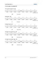
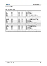
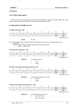
P1PU (P1 Pull-up Resistor Selection Register) : 96H
7
6
5
4
3
2
1
0
–
P16PU
P15PU
P14PU
P13PU
P12PU
P11PU
P10PU
–
R/W
R/W
R/W
R/W
R/W
R/W
R/W
Initial value : 00H
P1PU[6:0]
Configure Pull-up Resistor of P1 Port
0
Disable
1
Enable
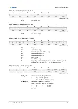
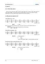
P1OD (P1 Open-drain Selection Register) : 95H
7
6
5
4
3
2
1
0
–
P16OD
P15OD
P14OD
P13OD
P12OD
P11OD
P10OD
–
R/W
R/W
R/W
R/W
R/W
R/W
R/W
Initial value : 78H
P1OD[6:0]
Configure Open-drain of P1 Port
0
Push-pull output
1
Open-drain output
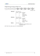
P1DB (P1 Debounce Enable Register) : A7H
7
6
5
4
3
2
1
0
–
–
P15DB
P14DB
P13DB
–
P11DB
P10DB
–
–
R/W
R/W
R/W
–
R/W
R/W
Initial value : 00H
P15DB
Configure Debounce of P15 Port
0
Disable
1
Enable
P14DB
Configure Debounce of P14 Port
0
Disable
1
Enable
P13DB
Configure Debounce of P13 Port
0
Disable
1
Enable
P11DB
Configure Debounce of P11 Port
0
Disable
1
Enable
P10DB
Configure Debounce of P10 Port
0
Disable
1
Enable
NOTES) 1. If the same level is not detected on enabled pin three or four times in a row at the sampling clock, the
signal is eliminated as noise.
2. A pulse level should be input for the duration of 3 clock or more to be actually detected as a valid
edge.
3. The port debounce is automatically disabled at stop mode and recovered after stop mode release.
Содержание MC96FM204
Страница 17: ...MC96FM204 FM214 April 7 2016 Ver 1 8 17 4 Package Diagram Figure 4 1 20 Pin SOP Package ...
Страница 18: ...MC96FM204 FM214 18 April 7 2016 Ver 1 8 Figure 4 2 20 Pin TSSOP Package ...
Страница 19: ...MC96FM204 FM214 April 7 2016 Ver 1 8 19 Figure 4 3 16 Pin SOP Package ...
Страница 20: ...MC96FM204 FM214 20 April 7 2016 Ver 1 8 Figure 4 4 16 Pin TSSOP Package ...

