


MC96FM204/FM214
April 7, 2016 Ver. 1.8
63
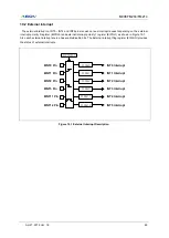
9.5 P2 Port
9.5.1 P2 Port Description
P2 is 2-bit I/O port. P2 control registers consist of P2 data register (P2), P2 direction register (P2IO), P2 pull-up
resistor selection register (P2PU) and P2 open-drain selection register (P2OD).
9.5.2 Register description for P2
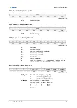
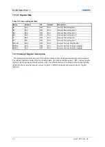
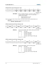
P2 (P2 Data Register) : 90H
7
6
5
4
3
2
1
0
–
–
–
–
–
–
P21
P20
–
–
–
–
–
–
R/W
R/W
Initial value : 00H
P2[1:0]
I/O Data
Note) Do not use the
“direct bit test and branch” instruction for input port, more detail information is at
Appendix B.
Example) Avoid direct input port bit test and branch condition as below
If(P20)
→
if(P2 & 0x01)
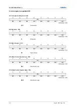
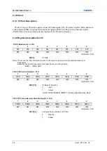
P2IO (P2 Direction Register) : 99H
7
6
5
4
3
2
1
0
–
–
–
–
–
–
P21IO
P20IO
–
–
–
–
–
–
R/W
R/W
Initial value : 00H
P2IO[1:0]
P2 Data I/O Direction
0
Input
1
Output
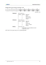
P2PU (P2 Pull-up Resistor Selection Register) : A1H
7
6
5
4
3
2
1
0
–
–
–
–
–
–
P21PU
P20PU
–
–
–
–
–
–
R/W
R/W
Initial value : 00H
P2PU[1:0]
Configure Pull-up Resistor of P2 Port
0
Disable
1
Enable
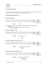
P2OD (P2 Open-drain Selection Register) : 9AH
7
6
5
4
3
2
1
0
–
–
–
–
–
–
P21OD
P20OD
–
–
–
–
–
–
R/W
R/W
Initial value : 00H
P2OD[1:0]
Configure Open-drain of P2 Port
0
Push-pull output
1
Open-drain output
Содержание MC96FM204
Страница 17: ...MC96FM204 FM214 April 7 2016 Ver 1 8 17 4 Package Diagram Figure 4 1 20 Pin SOP Package ...
Страница 18: ...MC96FM204 FM214 18 April 7 2016 Ver 1 8 Figure 4 2 20 Pin TSSOP Package ...
Страница 19: ...MC96FM204 FM214 April 7 2016 Ver 1 8 19 Figure 4 3 16 Pin SOP Package ...
Страница 20: ...MC96FM204 FM214 20 April 7 2016 Ver 1 8 Figure 4 4 16 Pin TSSOP Package ...