


YORK INTERNATIONAL
54
FORM 160.54-M1(503)
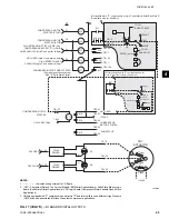
Display Interface Board
SECTION 6
DISPLAY INTERFACE BOARD
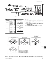
(REFER TO FIG. 28)
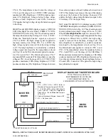
The
Display Interface Board
is located on the
Liq-
uid Crys tal Dis play
mount ing plate and is part of the
Microboard in ter face to the Display. It per mits the use
of Displays by dif fer ent man u fac tur ers, by pro vid ing the
Microboard with a means of au to mat i cal ly de ter min ing
which Dis play is present.
Since different Display manufacturers require dif fer ent
timing and control signals, the Display Controller on
the Microboard must be con
fi
gured to meet the re quire -
ments of the actual Display installed. When AC power
is applied to the OptiView Control Center, as part of the
power-up sequence, the Microboard reads the four Panel
ID wire jumpers, P1D0 through P1D3, on the
Dis play
In ter face Board
to de ter mine which Display is present.
The con
fi
g u ra tion of these jumpers in di cates the actual
Dis play that is in stalled on the OptiView Control Cen ter
door. The Display Con trol ler on the Microboard is then
con
fi
g ured ap pro pri ate ly.
On Sharp and NEC displays the con
fi
guration of wire
jump ers P30 and P31 de ter mines whether the Display
scan ori en ta tion is
Nor mal
or
Reverse
(im age re ver sal)
scan. As de scribed in the pre ced ing “Display” sec tion,
Nor mal scan is left to right, be gin ning with the top row
and con tinu ing se quen tial ly through the rows to the
bot tom row. Nor mal scan is used in OptiView Control
Cen ter ap pli ca tions. In Dis play applications oth er than
OptiView Control Cen ter ap pli ca tions, image re ver sal
is some times re quired. In im age reversal ap pli ca tions,
the scan is re versed; the scan is right to left, be gin ning
with the bot tom row and pro ceed ing to the top row. The
jump er con
fi
g u ra tions de ter mine the voltage level at Dis-
play In ter face Board J1-30 (P30) and J1-31 (P31). If P30
is IN, the voltage at J1-30 is +5.0VDC or +3.3VDC (as
de ter mined by po si tion of Microboard Pro gram Jump er
JP2); if OUT, 0VDC. If P31 is IN, the volt age at J1-31 is
GND; if OUT, 0VDC. The Display reads these volt ag es
and adopts a scan mode as fol lows:
SHARP LQ10D367 & LQ10D421 Displays:
SHARP displays require con
fi
guration of both jump ers
to achieve total image reversal.
P30 IN - Normal scan; left to right
OUT - Reverse scan: right to left
P31 IN - Normal scan; top to bottom
OUT - Re verse scan; bottom to top
NEC NL6448AC33-24 Display:
P30 Not Used
P31 IN or OUT - Normal scan; left to right, top to
bottom
The wire jumpers on this board are not
fi
eld con
fi
gu-
rable, as with typical Program Jumpers. There are two
vari a tions of the
Display Interface Board
. Each board
has the wire jumpers con
fi
gured ap pro pri ate ly for the
dis play to which it is attached, as shown below.
Display
Interface Boards
are avail able in di vid u al ly for ser vice
re place ment. The YORK part num ber of the Dis play
In ter face Board com pat i ble with the in stalled Dis play is
listed on a label at tached to the Dis play mount ing plate.
How ev er, ser vice re place ment Dis plays are pro vid ed as
a kit (331-01771-000) that in cludes, among oth er items,
the ap pro pri ate
Display In ter face Board
for the Dis-
play in clud ed in the kit. Re fer to ex pla na tion in “Liq uid
Crys tal Dis play” section.
031-01765-001:
Display applicability - LG Semicon LP104V2-W
&
NEC NL6448AC33-24
Jumper con
fi
guration - PID0 - IN
PID1 - OUT
PID2 - OUT
PID3 - OUT
P30 - OUT
P31 - OUT
031-01765-002:
Display applicability - SHARP LQ10D367 &
LQ10D421
Jumper con
fi
guration - PID0 - OUT
PID1 - IN
PID2 - OUT
PID3 - OUT
P30 - IN
P31 - IN
The red, green and blue display drive and control sig nals
are simply passed through the
Display Interface Board
.
The val ue of VCC is 5VDC or +3.3VDC, as
de ter mined by the position of Program Jump er JP2 on
the Microboard. PID0 through PID3, when in stalled,
con nect their re spec tive Microboard (J5) inputs to GND;
when re moved, the Microboard pulls these sig nals up
to +5VDC. When P30 is in stalled, the Display input
(CN1-30) is con nect ed to VCC (+5VDC or +3.3VDC
as de ter mined by Microboard Program Jump er JP2).
When P31 is installed, the Dis play input (CN1-31) is
con nect ed to GND.
Summary of Contents for MAXE OPTIVIEW YK
Page 28: ...YORK INTERNATIONAL 28 FORM 160 54 M1 503 Microboard FIG 7 MICROBOARD LD07776...
Page 60: ...YORK INTERNATIONAL 60 FORM 160 54 M1 503 Keypad FIG 32 KEYPAD CONNECTOR LD04074...
Page 61: ...FORM 160 54 M1 503 61 YORK INTERNATIONAL FIG 33 KEYPAD LD04075 LD04076 8...
Page 173: ...FORM 160 54 M1 503 173 YORK INTERNATIONAL 26 This page intentionally left blank...
Page 177: ...FORM 160 54 M1 503 177 YORK INTERNATIONAL 26 This page intentionally left blank...


