


ZCU102 Evaluation Board User Guide
37
UG1182 (v1.2) March 20, 2017
Chapter 3:
Board Component Descriptions
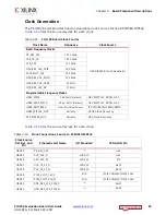
SD1 (MIO 39-51)
A PS-side interface to an SD card connector is provided for booting and file system storage.
This interface is used for the SD boot mode and supports SD3.0 access post boot.
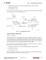
SD Card Interface
[
, callout 6]
The ZCU102 board includes a secure digital input/output (SDIO) interface to provide access
to general purpose non-volatile SDIO memory cards and peripherals. Information for the
SD I/O card specification can be found at the SanDisk Corporation
or SD
Association
websites. The ZCU102 SD card interface supports the SD1_LS
configuration boot mode documented in the
Zynq Ult MPSoC Technical Reference
Manual
(UG1085)
The SDIO signals are connected to XCZU9EG MPSoC PS bank 501 which has its V
CCMIO
set
to 1.8V. Each of the six MIOxx_SDIO_* nets has a series 30 ohm resistor at the source. An
NXP IP4856CX25 SD 3.0-compliant voltage level-translator U133 is present between the
XCZU9EG MPSoC and the SD card connector (J100). The NXP IP4856CX25 U133 device
provides SD3.0 capability with SDR104 performance. The NXP SD3.0 level shifter is mounted
on an Aries adapter board that has the pin mapping shown in
.
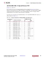
Table 3-9:
U133 IP4856CX25 Adapter Pin-Out
Aires Adapter
Pin Number
IP4856CX25 U133
Pin Number
IP4856CX25 U133
Pin Name
1
C1
CLK_IN
2
C3
GND
3
D3
CD
4
D2
CMD_H
5
E2
CLK_FB
6
E4
WP
7
B4
VLDO
8
C4
V
SD_REF
9
A3
DIR_0
10
A4
V
SUPPLY
11
B3
V
CCA
12
A2
DIR_CMD
13
D1
DATA0_H
14
B2
SEL
15
B1
DATA3_H
16
E1
DATA1_H


