


ZCU102 Evaluation Board User Guide
33
UG1182 (v1.2) March 20, 2017
Chapter 3:
Board Component Descriptions
Quad-SPI Flash Memory (MIO 0–12)
[
, callout 4]
The Micron dual MT25QU512ABB8ESF serial NOR flash Quad-SPI memories are capable of
holding the boot image for the MPSoC system. To achieve higher performance two
Quad-SPI devices are connected in parallel and provide an 8-bit data bus for booting and
configuration. This interface is used to support QSPI32 boot mode as defined in the
Zynq
Ult MPSoC Technical Reference Manual
(UG1085)
The dual Quad-SPI flash memory located at U119/U120 provides 1 Gb of non-volatile
storage that can be used for configuration and data storage.
• Part number: MT25QU512ABB8ESF-0SIT (Micron)
• Supply voltage: 1.8V
• Datapath width: 8 bits
• Data rate: Various depending on Single/Dual/Quad mode
The connections between the SPI flash memory and the XCZU9EG MPSoC are listed in
The configuration and Quad-SPI section of the
Zynq Ult MPSoC Technical Reference
Manual
(UG1085)
provides details on using the Quad-SPI flash memory. For more
QSPI details, see the Micron MT25QU512ABB8ESF-0SIT data sheet at the Micron website
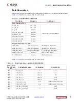
Table 3-6:
Quad-SPI Component Connections to FPGA U1
XCZU9EG
(U1) Pin
Net Name
Quad-SPI U119 (LWR), U120 (UPR)
Pin Number
Pin Name
AH16
MIO4_QSPI_LWR_DQ0
15
DQ0
AJ16
MIO1_QSPI_LWR_DQ1
8
DQ1
AD16
MIO2_QSPI_LWR_DQ2
9
DQ2_WP_B
AG16
MIO3_QSPI_LWR_DQ3
1
DQ3_RST_HOLD_B
AF16
MIO0_QSPI_LWR_CLK
16
C
AM15
MIO5_QSPI_LWR_CS_B
7
S_B
AE17
MIO8_QSPI_UPR_DQ0
15
DQ0
AP15
MIO9_QSPI_UPR_DQ1
8
DQ1
AH17
MIO10_QSPI_UPR_DQ2
9
DQ2_WP_B
AF17
MIO11_QSPI_UPR_DQ3
1
DQ3_RST_HOLD_B
AJ17
MIO12_QSPI_UPR_CLK
16
C
AD17
MIO7_QSPI_UPR_CS_B
7
S_B


