background image

Virtex-6 FPGA System Monitor

www.xilinx.com

49

UG370 (v1.1) June 14, 2010

Application Guidelines

analog power supply and ground reference are also routed into the center of the BGA 
using traces. No power planes are required to supply a ground reference for System 
Monitor. The analog supply and ground reference are connected to the external reference 
IC as shown in 

Figure 24, page 46

. In the PCB implementation shown in 

Figure 28

, the 

supply and ground traces are routed on either side of the reference traces on the same 
signal layer and act as guards between the reference traces and any potential aggressors 
(e.g., clocks and switching I/Os). It is not a requirement that the supply and ground traces 
are routed on the same signal layer as shown, but they should be routed on an adjacent 
layer. The V

REFN

 and AV

SS

 traces should be connected at (or close to) the ground pin of the 

reference IC. The ferrite bead that connects the analog ground trace to system ground 
should also be placed close to the reference IC. Also shown in 

Figure 28

 is the routing (from 

the top) of the dedicated analog input pair (V

P

 and V

N

). These inputs are also routed as a 

differential pair. 

The external reference IC should be placed as close as possible to the FPGA to reduce the 
opportunities for coupled noise and to minimize any impedances in the reference traces. 
The staggered via field also allows the 10 nF decoupling on V

REFP

 and AV

DD

 to be placed 

in the center of the array close to the package balls. V

REFP

 should be decoupled to V

REFN


and AV

DD

 to AV

SS 

near the package balls.

When using the on-chip reference, the layout of the PCB is greatly simplified. The V

REFP


and V

REFN

 pins should be shorted to AGND locally at the package balls - see 

Figure 24, 

page 46

. The ferrite beads used to separate AGND and digital GND should be placed close 

to the System Monitor balls in the center of the array along with a 10 nF decoupling 
capacitor for AV

DD

.

Figure 27

 an

Figure 28

 are only intended to guide a PC board implementation. If it is 

feasible to create an analog reference plane, then there is no issue with doing this. 
However, the reference inputs should still be routed as differential pairs as shown.

Example Instantiation of SYSMON

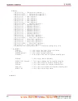
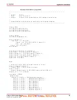
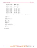
The following sample design is intended to illustrate a basic instantiation of the Virtex-6 
FPGA System Monitor in a design (refer to 

System Monitor Primitive, page 8

 for details on 

the System Monitor I/O and attributes). 

Figure 29

 illustrates a block diagram of the sample 

design. In this design, SYSMON is set up to monitor the V

CCAUX

 supply and generate an 

alarm on ALM[2], if the monitored supply moves outside the specified limits. The 
measured value of V

CCAUX

 can be checked at any time on the DO bus. The design requires 

an external clock to be provided. This design uses a 50 MHz external clock. 

Note:

Because an internal clock divider is provided, a clock in the range 2 MHz to 200 MHz can be 

used as a clock source. 

The BUSY signal is also brought out so the ADC conversion rate is easily monitored. The 
BUSY signal is also used to clock the DO data into a logic analyzer or other data acquisition 
system for inspection. By varying the V

CCAUX

 supply on the board, the alarm can be 

triggered or the varying supply voltage can be monitored on the DO bus.

www.BDTIC.com/XILINX

Summary of Contents for Virtex-6 FPGA

Page 1: ...Virtex 6 FPGA System Monitor User Guide UG370 v1 1 June 14 2010 www BDTIC com XILINX ...

Page 2: ... with technical support or assistance that may be provided to you in connection with the Information THE DOCUMENTATION IS DISCLOSED TO YOU AS IS WITH NO WARRANTY OF ANY KIND XILINX MAKES NO OTHER WARRANTIES WHETHER EXPRESS IMPLIED OR STATUTORY REGARDING THE DOCUMENTATION INCLUDING ANY WARRANTIES OF MERCHANTABILITY FITNESS FOR A PARTICULAR PURPOSE OR NONINFRINGEMENT OF THIRD PARTY RIGHTS IN NO EVEN...

Page 3: ...ncer Registers 48h to 4Fh 21 Alarm Registers 50h to 57h 21 DRP JTAG Interface 21 System Monitor DRP JTAG Write Operation 21 System Monitor JTAG DRP Read Operation 22 JTAG DRP Commands 23 DRP Arbitration 24 JTAGBUSY 24 JTAGMODIFIED 24 JTAGLOCKED 24 System Monitor Control Logic 25 Channel Sequencer 25 ADC Channel Selection 48h and 49h 26 ADC Channel Averaging 4Ah and 4Bh 27 ADC Channel Analog Input ...

Page 4: ...escription 41 Unipolar Input Signals 42 Bipolar Input Signals 43 Application Guidelines 45 Reference Inputs VREFP and VREFN 45 Analog Power Supply and Ground AVDD and AVSS 45 External Analog Inputs 47 Anti Alias Filters 47 PC Board Design Guidelines 47 Example Instantiation of SYSMON 49 SYSMON I O 50 SYSMON Attributes 51 Simulation of the SYSMON Design 57 EDK Support for System Monitor 59 ChipScop...

Page 5: ...or device package combinations and maximum I Os pin definitions pinout tables pinout diagrams mechanical drawings and thermal specifications Virtex 6 FPGA Configuration Guide This all encompassing configuration guide includes chapters on configuration interfaces serial and SelectMAP bitstream encryption boundary scan and JTAG configuration reconfiguration techniques and readback through the Select...

Page 6: ...e in all Virtex 6 FPGAs except the XC6VLX760 Virtex 6 FPGA DSP48E1 Slice User Guide This guide describes the architecture of the DSP48E1 slice in Virtex 6 FPGAs and provides configuration examples Virtex 6 FPGA PCB Design Guide This guide provides information on PCB design for Virtex 6 devices with a focus on strategies for making design decisions at the PCB and interface level Additional Support ...

Page 7: ...n monitoring features For example an automatic channel sequencer allows a user defined selection of parameters to be automatically monitored and user programmable averaging is enabled to ensure robust noise free measurements System Monitor also provides user programmable alarm thresholds for the on chip sensors Thus if an on chip monitored parameter moves outside the user specified operating range...

Page 8: ... see Automatic Alarms page 29 All System Monitor features are customizable at run time through the Dynamic Reconfiguration Port DRP and the System Monitor control registers These control registers can also be initialized at design time when System Monitor is instantiated in a design see Register File Interface page 14 For the latest information including FAQs software updates and tutorials refer t...

Page 9: ...hat provide a differential analog input When designing with the System Monitor feature but not using the dedicated external channel of VP and VN the user should connect both VP and VN to the analog ground VAUXP 15 0 VAUXN 15 0 Inputs Sixteen auxiliary analog input pairs In addition to the dedicated differential analog input System Monitor uses 16 differential digital input pairs as low bandwidth d...

Page 10: ...using the JTAG TAP However System Monitor only operates in safe mode during configuration and the contents of the System Monitor control registers JTAGLOCKED 1 Output Used to indicate that a DRP port lock request has been made by the Joint Test Action Group JTAG interface see DRP Arbitration page 24 JTAGMODIFIED 1 Output Used to indicate that a JTAG Write to the DRP has occurred JTAGBUSY 1 Output ...

Page 11: ...gure 4 For more information regarding power supply requirements see Application Guidelines page 45 Analog to Digital Converter The ADC is used to digitize the output of the on chip sensors and voltages connected to the external analog inputs The ADC specifications are listed in the Virtex 6 FPGA Data Sheet The System Monitor ADC carries out a 16 bit resolution conversion of all sensor and external...

Page 12: ...ed power supply connections and PC Board layout see Application Guidelines page 45 In addition to on chip sensors the ADC is used to digitize external analog signals There is one dedicated analog input pin pair and 16 user programmable analog input pairs supplied for this purpose The ADC has a true differential sampling analog input scheme allowing the ADC to achieve a high degree of accuracy when...

Page 13: ...ature reading is placed in the output data registers at address 00h on the DRP see Register File Interface page 14 The full ADC transfer function describes temperatures outside the FPGA operating temperature range This does not mean that the FPGA is operational at these temperatures refer to Virtex 6 FPGA Data Sheet for temperature specifications System Monitor is operational over a temperature ra...

Page 14: ...Status Registers page 15 Register File Interface Figure 7 illustrates the System Monitor register file interface All registers in the register file interface are accessible through the DRP The DRP can be accessed via a fabric port or the JTAG TAP Access is governed by an arbitrator see DRP Arbitration page 24 The DRP allows the user to access up to 128 16 bit registers DADDR 6 0 00h to 7Fh from th...

Page 15: ...us registers and definitions X Ref Target Figure 7 Figure 7 System Monitor Register Interface DI 15 0 DO 15 0 DADDR 6 0 DCLK JTAGBUSY JTAGLOCKED JTAGMODIFIED DWE DEN DRDY Config Reg 0 40h Config Reg 1 41h Config Reg 2 42h Test Reg 1 44h Test Reg 0 43h Test Reg 4 47h Test Reg 2 45h Test Reg 3 46h Alarm Reg 0 50h Alarm Reg 1 51h Alarm Reg 2 52h Alarm Reg 4 54h Alarm Reg 3 53h Alarm Reg 7 57h Alarm R...

Page 16: ...e reference input VREFP is stored in this register The 10 MSBs correspond to the ADC transfer function shown in Figure 6 The supply sensor is used when measuring VREFP This channel is also used during a calibration see System Monitor Calibration page 31 Undefined 06h to 07h These locations are unused and contain invalid data Supply Offset 08h The calibration coefficient for the supply sensor offse...

Page 17: ... are illustrated in Figure 9 The Xs in Figure 9 define these bit positions as don t cares Bits 0 1 and 2 in configuration register 2 42h should always be set to 0 The configuration registers are modifiable through the DRP after the FPGA has been configured For example a soft microprocessor or state machine can be used to alter the contents of the System Monitor control registers at any time during...

Page 18: ...Config Reg 1 DADDR 6 0 41h Config Reg 2 DADDR 6 0 42h Config Reg 0 DADDR 6 0 40h DI0 DI1 DI2 DI3 DI4 DI5 DI6 DI7 DI8 DI9 DI10 DI11 DI12 DI13 DI14 DI15 CH4 CH3 CH2 CH1 CH0 ACQ X X X X X CAVG AVG1 AVG0 BU EC UG370_09_060809 DI12 DI13 DI14 DI15 DI0 DI1 DI2 DI3 DI4 DI5 DI6 DI7 DI8 DI9 DI10 DI11 ALM0 ALM1 ALM2 OT SEQ1 SEQ0 X X X X X X CAL0 CAL1 CAL2 CAL3 DI12 DI13 DI14 DI15 DI0 DI1 DI2 DI3 DI4 DI5 DI6 ...

Page 19: ...for the bit assignments see Table 9 CAL0 to CAL3 These bits are used to enable the application of the calibration coefficients to the ADC and on chip supply sensor measurements see System Monitor Calibration page 31 A logic 1 enables calibration and a logic 0 disables calibration For bit assignments see Table 10 CD0 to CD7 These bits are used to select the division ratio between the DRP clock DCLK...

Page 20: ...fe mode see Pre Configuration Operation page 10 0 1 One pass through sequence 1 0 Continuous cycling of sequence 1 1 Single Channel mode Sequencer Off Table 10 Calibration Enables Name Description CAL0 ADC offset correction enable CAL1 ADC offset and gain correction enable CAL2 Supply Sensor offset correction enable CAL3 Supply Sensor offset and gain correction enable Table 11 DCLK Division Select...

Page 21: ...ruction register IR must first be loaded with the SYSMON instruction The Controller is first placed in the IR scan mode and the SYSMON instruction is shifted to the IR After the SYSMON instruction is loaded all data register DR scan operations are carried out on the SYSMON DR When the data shifted into SYSMON DR is a JTAG DRP Write command the SYSMON DRP arbitrator carries out a DRP write The form...

Page 22: ...itrator enough time to fetch the System Monitor DRP data As mentioned previously if the DCLK frequency is significantly faster than the TCK these idle states might not be required Note Implementing a DR scan operation before the arbitrator has completed the DRP read operation results in old DRP data being transferred to the SYSMON DR during the DR capture phase To ensure reliable operation over al...

Page 23: ...AG DRP Read Operation TCK TMS TDI TDO Idle to allow DRP Read to complete before shifting out result Idle to allow DRP Read to complete before shifting out result 0 31 30 MSB MSB LSB LSB Old DRP Write or New Read Data shfited out Read Command shifted into SYSMON DR 0 31 30 MSB MSB LSB LSB New DRP Read Data shifted out Read Command shifted into SYSMON DR RTI UIR RTI RTI RTI RTI RTI RTI DRS CDR SDR S...

Page 24: ...h the interconnect when the JTAG port is also being used JTAGBUSY This signal becomes active during the update phase of a DRP transaction through the JTAG TAP The signal resets when the JTAG SYSMON DR transaction is completed Each Read Write to the SYSMON DR is treated as an individual transaction If DRP access initiates through the interconnect port when JTAGBUSY is High then the arbitrator queue...

Page 25: ... The Channel Sequencer provides a method for the user to set up a predefined sequence of channels both internal and external to be automatically monitored The Channel Sequencer function is implemented using eight control registers from address 48h to 4Fh on the DRP see Control Registers page 17 These eight registers can be viewed as four pairs of 16 bit registers Each pair of registers controls on...

Page 26: ...gister 48h and ending with the MSB bit 15 of register 49h Table 13 Sequencer ADC Channel Selection Control Register 48h Sequence Number Bit ADC Channel Description 1 0 8 System Monitor calibration 1 1 9 Invalid channel selection 2 10 3 11 4 12 5 13 6 14 7 15 2 8 0 On Chip temperature 3 9 1 Average On Chip VCCINT 4 10 2 Average On Chip VCCAUX 5 11 3 VP VN Dedicated analog inputs 6 12 4 VREFP 1 25V ...

Page 27: ...egister will be updated for every pass through the sequencer When a channel has averaging enabled its status register is only updated after the averaging is complete An example sequence is Temperature and VAUX 1 and averaging of 16 is enabled on VAUX 1 The sequence will be Temperature VAUX 1 Temperature VAUX 1 Temperature VAUX 1 for each of the conversions where the temperature status register is ...

Page 28: ...DC Channel Description 0 16 Enable averaging VAUXP 0 VAUXN 0 Auxiliary channel 1 1 17 Enable averaging VAUXP 1 VAUXN 1 Auxiliary channel 2 2 18 Enable averaging VAUXP 2 VAUXN 2 Auxiliary channel 3 3 19 Enable averaging VAUXP 3 VAUXN 3 Auxiliary channel 4 4 20 Enable averaging VAUXP 4 VAUXN 4 Auxiliary channel 5 5 21 Enable averaging VAUXP 5 VAUXN 5 Auxiliary channel 6 6 22 Enable averaging VAUXP 6...

Page 29: ...e DRP Status registers starting at address 20h see Status Registers page 15 On power up or after reset all the minimum registers are set to FFFFh and the maximum registers are set to 0000h Each new measurement generated for an on chip sensor is compared to the contents of its maximum and minimum registers If the measured value is greater than the contents of its maximum registers then the measured...

Page 30: ... is enabled the OT signal can be used to trigger a device power down When OT goes active High the FPGA enters power down approximately 10 ms later The power down feature initiates a configuration shutdown sequence disabling the device when finished and asserts GHIGH to prevent any contention see Virtex 6 FPGA Configuration Guide When OT is deasserted GHIGH will also deassert and the startup sequen...

Page 31: ...ex 6 FPGAs The thermal diode can be accessed by using the DXP and DXN pins in bank 0 The thermal diode is independent of System Monitor and its use in no way affects the System Monitor operation If the thermal diode is not being used these pins should be tied to ground The thermal diode has a non ideality factor of 1 0002 and a series resistance of 2 Ω For implementation details consult the data s...

Page 32: ...sitive If it is 0 then the correction factor is negative The next five bits store the magnitude of the gain correction factor Each bit is equivalent to 0 1 For example if the ADC has a positive gain error of 1 see Figure 13 page 33 then the gain calibration coefficient records 1 the 1 correction applied to cancel the 1 error Since the correction factor is negative the sixth bit is set to zero The ...

Page 33: ...ystem Monitor is operated in one of two possible timing modes continuous sampling mode and event driven sampling mode In continuous sampling mode the ADC automatically starts a new conversion at the end of a current conversion cycle In event sampling mode the user must initiate the next conversion after the current conversion cycle ends by using the CONVST or CONVSTCLK inputs The operating mode is...

Page 34: ...selected input channel source impedance The acquisition time is nominally four ADCCLKs in duration from the end of the previous conversion phase to the sampling edge of the next conversion phase see Figure 14 When operating in Single Channel mode the user must write to configuration 0 to select the next channel for conversion Write operations to the configuration registers to select the next chann...

Page 35: ...ing operated in sequence mode the user identifies the channel being converted by monitoring the channel address CHANNEL 4 0 logic outputs The multiplexer channel address of the channel being converted is updated on these logic outputs when BUSY transitions Low at the end of the conversion phase The channel address outputs can be used with the EOC and DRDY signals to automatically latch the content...

Page 36: ...nstant is controlled by CONVST CONVSTCLK Therefore the acquisition time on a selected channel is also controlled by the CONVST CONVSTCLK CONVST and CONVSTCLK are logically OR ed within System Monitor If a long acquisition time is required then the user must leave the required acquisition time before CONVST CONVSTCLK is pulsed After the analog input has been sampled by a rising edge on CONVST CONVS...

Page 37: ...an internal clock used by the ADC X Ref Target Figure 15 Figure 15 Event Driven Sampling Mode Timing EOC EOS DCLK 1 84 85 96 1 2 21 20 19 18 ADCCLK Acquisition Time Conversion Time BUSY CONVST CHANNEL 4 0 N 1 Channel Selection N Selection Nth Conversion Finished Nth Sampling Edge UG370_15_060809 www BDTIC com XILINX ...

Page 38: ...9 describes the timing events shown in Figure 16 X Ref Target Figure 16 Figure 16 System Monitor Detailed Timing t5 t9 t8 t10 t7 t6 t4 t2 t1 t3 DCLK 1 2 3 4 5 DWE DEN DADDR 6 0 DI 15 0 DO 15 0 DRDY t11 t11 t13 t14 t14 t15 t12 t12 EOC EOS ALM 2 0 OT BUSY CHANNEL 4 0 UG370_16_060809 www BDTIC com XILINX ...

Page 39: ... Minimum DRP address set up time before rising edge of DCLK t7 Minimum DRP address hold time after rising edge of DCLK t8 Minimum DRP input data bus set up time before rising edge of DCLK t9 Minimum DRP input data bus hold time after rising edge of DCLK t10 Maximum DRP DCLK to DO delay access time 4 t11 Maximum delay on DRDY going High Low after a rising edge on DCLK t12 Maximum delay on EOC EOS g...

Page 40: ...t channels in preconfiguration operation a 1 must be written to bit 0 of the register at address 02h VCCAUX status register in the System Monitor register file interface The internal mapping in the System Monitor enables the auxiliary channels using the JTAG interface The auxiliary analog inputs are automatically enabled when System Monitor is instantiated in a design and these inputs are connecte...

Page 41: ...d acquisition time The acquisition time can be increased by reducing the ADCCLK frequency or setting the ACQ bit In the latter case the acquisition time is increased to 1 92 µs ten ADCCLK cycles and the conversion rate would be reduced to 162 5 kSPS for the same ADCCLK frequency In Event Timing Mode the user initiates the conversion cycle by using CONVST or CONVSTCLK allowing more control over the...

Page 42: ...ust be operated in a unipolar input mode This mode is selected by writing to configuration register 0 When unipolar operation is enabled the differential analog inputs VP VN have an input range of 0V to 1 0V In this mode the voltage on VP measured with respect to VN must always be positive Figure 19 shows a typical application of unipolar mode The VN input is typically connected to a local ground ...

Page 43: ...ing to configuration register 0 All input voltages must be positive with respect to analog ground AVSS When bipolar operation is enabled the differential analog input VP VN can have a maximum input range of 0 5V The common mode or reference voltage should not exceed 0 5V in this case see Figure 21 At a maximum common mode voltage of 1V on VN the differential analog input VP VN should not exceed 10...

Page 44: ...ment and is intended to indicate the sign of the input signal on VP relative to VN The designed code transitions occur at successive integer LSB values that is 1 LSB 2 LSBs 3 LSBs etc The LSB size in volts is equal to 1V 210 or 1V 1024 0 977 mV The ideal transfer function is illustrated in Figure 23 X Ref Target Figure 22 Figure 22 Bipolar Signals X Ref Target Figure 23 Figure 23 Bipolar Transfer ...

Page 45: ...ut using the decoupling capacitors recommended in the reference IC data sheet The recommended reference connections are illustrated in Figure 24 The System Monitor also has an on chip reference which is selected by connecting VREFP and VREFN to AGND as shown in Figure 24 Due to reduced accuracy the on chip reference does impact the measurement performance of the System Monitor as explained in this...

Page 46: ...haves like a resistor at high frequencies and functions as a lossy inductor A typical ferrite impedance vs frequency plot is shown in Figure 25 The ferrite helps provide high frequency isolation between digital and analog grounds The reference IC maintains a 1 25V difference of between VREFP and VREFN The ferrite offers little resistance to the analog DC return current X Ref Target Figure 24 Figur...

Page 47: ...coupled differential pairs Anti Alias Filters Also shown in Figure 26 is a low pass filter network at the analog differential inputs This filter network is commonly referred to as the anti alias filter and should be placed as close as possible to the package pins The sensor can be placed remotely from the package as long as the differential input traces are closely coupled The anti alias filter at...

Page 48: ...differential pair from an external 1 25V reference IC at the bottom edge of the FPGA refer to Figure 24 page 46 for the connections The X Ref Target Figure 27 Figure 27 Routing Channels to Center of Array Created by Staggering Vias X Ref Target Figure 28 Figure 28 Reference Inputs VREFP and VREFN should be Routed as Differential Pairs into the Center of the BGA UG370_27_060809 UG370_28_060809 www ...

Page 49: ...he package balls When using the on chip reference the layout of the PCB is greatly simplified The VREFP and VREFN pins should be shorted to AGND locally at the package balls see Figure 24 page 46 The ferrite beads used to separate AGND and digital GND should be placed close to the System Monitor balls in the center of the array along with a 10 nF decoupling capacitor for AVDD Figure 27 and Figure ...

Page 50: ...corresponding register is placed on the DO 15 0 bus In this example DEN is connect to EOS DWE Input DRP write enable Since no writes take place to the DRP this input is held at logic 0 RESET Input SYSMON reset signal It is tied to logic 0 in this example CHANNEL 4 0 Output ADC input multiplexer address The ADC input multiplexer address is placed on this bus at the end of the conversion when BUSY t...

Page 51: ...UX supply measurement alarm The Alarm limits are set to 2 5 5 in this example 2 375V and 2 625V When the supply moves outside these limits ALM 2 goes active High The output resets to Low again after the measured VCCAUX supply is inside the limits Table 20 SYSMON I Os Cont d Name I O Description Table 21 SYSMON Attributes Attribute Setting Description INIT_40 1000h Set averaging to 16 AVG1 0 AVG0 1...

Page 52: ...old for VCCAUX is generated from the transfer function for the power supply sensor as shown in Figure 6 page 14 The limit can be calculated as Limit 3V 216 Therefore 2 625 3 216 57344 or E000h The value of the top 10 bits is 380h refer to Figure 6 INIT_56 CAAAh The lower alarm threshold for VCCAUX is also generated from the transfer function for the power supply sensor as shown in Figure 6 The lim...

Page 53: ...DCLK is needed to access the DRP The ALARM and BUSY signal remains active however The result in status register 2 VCCAUX can be accessed via the JTAG TAP refer to DRP JTAG Interface page 21 Author Xilinx Date July 11th 2007 Design Virtex 6 FPGA System Monitor Verilog example instantiation System Monitor instantiation by hand using the Language Template timescale 1ns 1 ps module v5_sysmon Inputs cl...

Page 54: ...egister 0 INIT_51 16 h0 Alarm limit register 1 INIT_52 16 hE000 Alarm limit register 2 INIT_53 16 h0 Alarm limit register 3 INIT_54 16 h0 Alarm limit register 4 INIT_55 16 h0 Alarm limit register 5 INIT_56 16 hCAAA Alarm limit register 6 INIT_57 16 h0 Alarm limit register 7 SIM_MONITOR_FILE vccaux_alarm txt Simulation analog entry file my_sysmon ALM alm 3 bit output for temp Vccint and Vccaux BUSY...

Page 55: ...is signal dobus std_logic_vector 15 downto 0 signal channel_int std_logic_vector 6 downto 0 signal channel std_logic_vector 4 downto 0 signal alm std_logic_vector 2 downto 0 signal eos std_logic begin bring out 10 bit MSB justified version of DO bus Vccaux dobus 15 downto 6 Connect ALM 2 Vccaux alarm to output alarm alm 2 Connect channel output to DRP DADDR inputs and set MSBs to 0 channel_int 00 ...

Page 56: ...arm limit register 1 INIT_52 X E000 Alarm limit register 2 INIT_53 X 0000 Alarm limit register 3 INIT_54 X 0000 Alarm limit register 4 INIT_55 X 0000 Alarm limit register 5 INIT_56 X CAAA Alarm limit register 6 INIT_57 X 0000 Alarm limit register 7 SIM_MONITOR_FILE vccaux_alarm txt Stimulus file for analog simulation port map DCLK clk DWE 0 DEN eos DADDR channel_int DO dobus CHANNEL channel EOS eo...

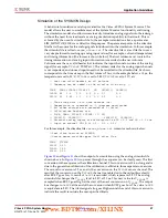
Page 57: ...l columns Comments can be added to the stimulus file using TIME TEMP VCCAUX VCCINT VP VN VAUXP 0 VAUXN 0 00000 45 2 5 1 0 0 5 0 0 0 7 0 0 05000 85 2 45 1 1 0 3 0 0 0 2 0 0 Time stamp data is in nano seconds ns Temperature is recorded in C degrees centigrade All other channels are recorded as V Volts Valid column headers are TIME TEMP VCCAUX VCCINT VP VN VAUXP 0 VAUXN 0 VAUXP 15 VAUXN 15 External a...

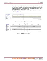
Page 58: ...d the data is placed on the bus four DCLK cycles after EOS DEN is pulsed The DRDY signal goes High to indicate valid data is on the bus Notice how the alarm signal goes High before the EOS signal is pulsed The VHDL and Verilog projects for this example can be downloaded from the Xilinx website at ug192 zip X Ref Target Figure 30 Figure 30 Simulation of System Monitor Design UG370_30_060809 X Ref T...

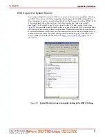
Page 59: ...ickly developed The System Monitor IP can be found in the IP Catalog under Analog see Figure 32 It is possible to use System Monitor as a general purpose ADC in an application by disabling the monitoring of the on chip sensors The basic System Monitor functionality can also be extended by the processor to include custom functionality and support various communication protocols for system managemen...

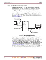
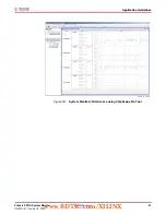
Page 60: ...o tool version 8 2 04 and later This tool automatically detects the presence of System Monitor on the JTAG chain and allow users to display the measurement data There is also a data logging function that allows users to record sensor readings along with time stamp information in a log file for analysis Users can also configure the System Monitor operation via JTAG using the ChipScope Pro tool by w...

Page 61: ...6 FPGA System Monitor www xilinx com 61 UG370 v1 1 June 14 2010 Application Guidelines X Ref Target Figure 34 Figure 34 System Monitor JTAG Access using ChipScope Pro Tool UG370_34_060809 www BDTIC com XILINX ...

Page 62: ...62 www xilinx com Virtex 6 FPGA System Monitor UG370 v1 1 June 14 2010 Application Guidelines www BDTIC com XILINX ...

Reviews: