


30
SP305 Spartan-3 Development Platform User Guide
www.xilinx.com
UG216 (v1.1) March 3, 2006
SP305 Spartan-3 Development Platform User Guide
R
DDR Loop Signal
The DDR loop signal is a trace driven and then received back at the FPGA with a delay
equal to the sum of the trace delays of the clock and DQS signals. This looped trace can be
used in high-speed memory controllers to help compensate for the physical trace delays
between the FPGA and DDR chips.
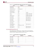
ZBT Synchronous SRAM (37)
The ZBT synchronous SRAM (Cypress CY7C1354B) provides high-speed, low-latency
external memory to the FPGA. The memory is organized as 256K x 36 bits, thereby
providing for a 32-bit data bus with support for four parity bits.
Note:
The SRAM and FLASH memory share the same data bus.
Table 2-29:
SRAM
Label
FPGA Pin
Description
SRAM_FLASH_D0
AD25
SRAM_FLASH_D1
AB22
SRAM_FLASH_D2
AC22
SRAM_FLASH_D3
AE24
SRAM_FLASH_D4
AF24
SRAM_FLASH_D5
AD23
SRAM_FLASH_D6
AE23
SRAM_FLASH_D7
AF23
SRAM_FLASH_D8
AD22
SRAM_FLASH_D9
AE22
SRAM_FLASH_D10
AF22
SRAM_FLASH_D11
AB21
SRAM_FLASH_D12
AC21
SRAM_FLASH_D13
AD21
SRAM_FLASH_D14
AE21
SRAM_FLASH_D15
AF21
SRAM_FLASH_D16
AB20
SRAM_FLASH_D17
AC20
SRAM_FLASH_D18
AE20
SRAM_FLASH_D19
AF20
SRAM_FLASH_D20
AA20
SRAM_FLASH_D21
Y19
SRAM_FLASH_D22
AA19


