


12
SP305 Spartan-3 Development Platform User Guide
www.xilinx.com
UG216 (v1.1) March 3, 2006
SP305 Spartan-3 Development Platform User Guide
R
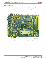
The FPGA and Platform Flash memory can be configured through the JTAG port. The
JTAG chain of the board is illustrated in
Figure 2-5
.
The chain starts at the PC4 connector and goes through the Platform Flash memory, the
FPGA, and an optional extension of the chain to the expansion card. Jumper J26 determines
if the JTAG chain should be extended to the expansion card.
The JTAG chain can be used to program the FPGA and access the FPGA for hardware and
software debug. The JTAG chain is also used to program the Platform Flash memory.
The PC4 JTAG connection to the JTAG chain allows a host PC to download bitstreams to
the FPGA using the iMPACT software tool. PC4 also allows debug tools such as the
ChipScope™ Pro Analyzer or a software debugger to access the FPGA.
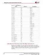
Configuration Address and Mode DIP Switches (13)
This 3-position DIP switch controls the configuration address and FPGA configuration
mode.
The three switches choose one of eight possible configuration addresses. It provides the
The Platform Flash memory supports up to four different images.
The three rightmost DIP switches set the FPGA configuration mode pins M2, M1, and M0
as shown in
Table 2-8
.
M2
M1
M0
Mode
Master Serial
Slave Serial
Master Parallel (SelectMAP)
Slave Parallel (SelectMAP)
JTAG
FPGA HSWAP_EN (14)
The default for the Spartan3 FPGA is to have an internal weak pull-up enabled on the
HSWAP_EN FPGA pin. The jumper J37 is used to control if a weak pull-up is present on
the user I/O during configuration. When there is no jumper on J37, a weak pull-up is
applied to the HSWAP_EN pin. The effect will be to disable internal pull-ups on User I/O
during configuration. If a jumper is placed on J37, the HSWAP_EN pin will be grounded.
Figure 2-5:
JTAG Chain
PC4
TDI
TDO
TDI
TDO
Pl
a
tFl
as
h
FPGA
TDI
TDO
Exp
a
n
s
ion
u
g216_05_101105
Table 2-8:
Configuration Mode DIP Switch Settings
0
0
0
1
1
1
0
1
1
1
1
0
1
0
1


