


22
SP305 Spartan-3 Development Platform User Guide
www.xilinx.com
UG216 (v1.1) March 3, 2006
SP305 Spartan-3 Development Platform User Guide
R
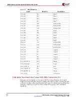
Differential Clock Input And Output With SMA Connectors (31)
High-precision clock signals can be input to the FPGA using differential clock signals
brought in through 50
Ω
SMA connectors, thereby allowing an external function generator
or other clock source to drive the differential clock inputs that directly feed the global clock
input pins of the FPGA. The FPGA can be configured to present a 100
Ω
termination
impedance.
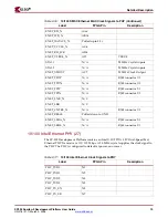
VGA_B4
K1
Blue 4
VGA_B5
K2
Blue 5
VGA_B6
K3
Blue 6
VGA_B7
K4
Blue 7
VGA_R0
H11
4.7K to GND
VGA_R1
B10
4.7K to GND
VGA_R2
A10
4.7K to GND
VGA_R3
H3
Red 3
VGA_R4
H4
Red 4
VGA_R5
J6
Red 5
VGA_R6
H5
Red 6
VGA_R7
G1
Red 7
VGA_G0
G11
4.7K to GND
VGA_G1
F11
4.7K to GND
VGA_G2
E11
4.7K to GND
VGA_G3
J5
Green 3
VGA_G4
K7
Green 4
VGA_G5
J7
Green 5
VGA_G6
H1
Green 6
VGA_G7
H2
Green 7
VGA_BLANK_N
H12
Blank
VGA_PSAVE_N
G12
Psave
VGA_SYNC_N
H13
Sync
VGA_VSYNC_N
D1
Vsync
VGA_HSYNC_N
E4
Hsync
VGA_CLK
F6
VGA clock
Table 2-21:
VGA FPGA Pins
Label
FPGA Pin
Description


