


SP305 Spartan-3 Development Platform User Guide
23
UG216 (v1.1) March 3, 2006
www.xilinx.com
Detailed Description
R
A differential clock output from the FPGA is driven out through a second pair of SMA
connectors; thereby allowing the FPGA to drive a precision clock to an external device such
as a piece of test equipment.
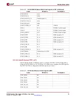
Table 2-22
summarizes the differential SMA clock pin
connections.
Label
Clock Name
FPGA Pin
SMA_DIFF_CLK_IN_N
SMA_DIFF_CLK_IN_P
SMA_DIFF_CLK_OUT_N
SMA_DIFF_CLK_OUT_P
Expansion Headers (32)
The board contains expansion headers for easy expansion or adaptation of the board for
other applications. The expansion connectors use standard 0.1" headers. The expansion
connectors contain connections to single-ended and differential FPGA I/Os, ground,
2.5V/3.3V/5V power, JTAG chain, and the IIC bus.
Differential Expansion I/O Connectors
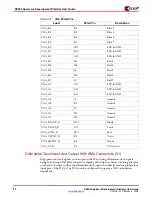
Header J5 contains 16 pairs of differential signal connections to the FPGA I/Os. This
permits the signals on this connector to carry high-speed differential signals such as LVDS
data. All differential signals are routed with 100
Ω
differential trace impedance. Matched
length traces are used across all differential signals. Because the differential signals connect
to the FPGA I/O, they may also be used as independent single-ended nets. The VCCIO of
these signals can be set to 2.5V or 3.3V by setting jumper J16.
Table 2-23
summarizes the
differential connections on this expansion I/O connector.
Table 2-22:
Differential SMA Clock Connections
J10
B13
J7
A13
J8
E1
J9
E2
Table 2-23:
Expansion I/O Differential Connections (J5)
Header Pin
(Diff Pair
Neg)
Label
(Diff Pair
Neg)
FPGA Pin
(Diff Pair
Neg)
Header Pin
(Diff Pair
Pos)
FPGA Pin
(Diff Pair
Pos)
Label
(Diff Pair
Pos)
J5, Pin 2
HDR2_2
U20
J5, Pin 4
V20
HDR2_4
J5, Pin 6
HDR2_6
V21
J5, Pin 8
W22
HDR2_8
J5, Pin 10
HDR2_10
W26
J5, Pin 12
W25
HDR2_12
J5, Pin 14
HDR2_14
T20
J5, Pin 16
T19
HDR2_16
J5, Pin 18
HDR2_18
P22
J5, Pin 20
P21
HDR2_20
J5, Pin 22
HDR2_22
AC26
J5, Pin 24
AC25
HDR2_24
J5, Pin 26
HDR2_26
Y21
J5, Pin 28
Y20
HDR2_28
J5, Pin 30
HDR2_30
AB26
J5, Pin 32
AB25
HDR2_32
J5, Pin 34
HDR2_34
W21
J5, Pin 36
W20
HDR2_36
J5, Pin 38
HDR2_38
AA22
J5, Pin 40
AA21
HDR2_40
J5, Pin 42
HDR2_42
AB24
J5, Pin 44
AB23
HDR2_44


