background image

cyber

®

 reaction wheel 2 


Project planning guide


Revision: 02 

Doc. no.: 5022-D060586 

en-33 

3.4.3.1  I2C interface 

The I2C bus is a master/slave bus system. The controlling microcontroller acts as the master, the 
different cyber

® 

reaction wheels 2 as slaves. 

The I2C interface is based on two lines. The clock line (SCL) and the data line (SDA) of the 
master are connected with all cyber

® 

reaction wheel 2 to I2C_SCL or I2C_SDA of customer 

interface B (see table 11) of the starter kit or the interface for reaction wheel D, see table 13. 
 
I2C clock frequency: 
The I2C master can be used in standard mode (= 100 kHz) and in fast mode (= 400 kHz). 
 
I2C addressing: 
The cyber

® 

reaction wheel 2 uses 7 bits for addressing. The default address is 0x77 (119 dec). 

This must be changed by the user during startup with the help of the cyber

® 

reaction wheel 

assistant as described in section 2.3.4.1 so that, for example, after a firmware update 
(see section 3.6), no address is used twice in the network. The address can also be changed with 
the Wittenstein software stack with ADCS without any problems. For synchronous setpoint 
transmission, please observe the information in the introduction of this chapter. 
 

3.4.3.2  SPI interface 

The SPI bus is a master/slave bus system. The controlling microcontroller acts as the master, the 
different cyber

® 

reaction wheels 2 as slaves. 

The SPI interface is based on four lines. The two data lines (MOSI, MISO) and the clock line 
(SCK) are star-wired to the various reaction wheels 2 to SPI_MOSI, SPI_MISO and SPI_SCK at 
customer interface B, table 11, of the starter kit or the interface to reaction wheel D, table 13. 
 
The chip select line (nCS) is used for data transmission by the microcontroller of the selected 
cyber

® 

reaction wheel 2. This is why each cyber

® 

reaction wheel 2 has its own chip select line. 

This line is connected to SPI_nCS of the customer interface B, table 11, the starter kit or the 
interface to reaction wheel D, table 13. 
 
SPI clock frequency: 
The SPI should use a clock frequency of at least 1 MHz. The maximum permitted clock frequency 
is 10 MHz. 
 
SPI settings, see figure 1.22: 
Mode: 

Full-Duplex Master 

Frame format: 

Motorola 

Data size: 

8 bits 

First bit: 

MSB (=highest bit) first 

Clock Polarity (CPOL): 

Clock Phase (CPHA): 


Summary of Contents for cyber reaction wheel 2

Page 1: ...Doc no 5022 D060586 Revision 02 cyber reaction wheel 2 Project planning guide...

Page 2: ...on please contact our support hotline WITTENSTEIN cyber motor GmbH support hotline Tel 49 0 79 31 493 14800 In the event of technical malfunctions contact us at the following address WITTENSTEIN cyber...

Page 3: ...heel assistant 23 2 3 1 Installation of the cyber reaction wheel assistant 23 2 3 2 CHM Help 23 2 3 3 Oscilloscope 23 2 3 4 Setting of communication parameters 24 2 3 4 1 Setting the I2C address 24 2...

Page 4: ...therefore void The operator must ensure that this operating manual is read through by all persons assigned to install operate or maintain the drive system and that they fully comprehend its content S...

Page 5: ...lly sensitive device 1 3 Structure of the safety information Safety information in this manual has been structured according to the following template Explanatory text shows the consequences of disreg...

Page 6: ...n wheel 2 Following the product specifications of the cyber reaction wheel 2 the cyber reaction wheel starter kit and the cyber reaction wheel assistant are the chapter on startup working with the rea...

Page 7: ...mentum range can be done without any limitations Intuitive startup and integration of the drive system is made possible by the cyber reaction wheel starter kit with the PC based graphical user interfa...

Page 8: ...cyber reaction wheel 2 Customized deviations are permissible The Data Matrix code DMC under the name plate is in the format C18x18 according to ECC200 It contains the Service Portal Address including...

Page 9: ...n with recuperation rev s 60 Max deceleration without recuperation rev s 30 Weight g 30 Max static imbalance gmm 0 02 Max dynamic imbalance gmm 0 2 Table 3 System characteristics of cyber reaction whe...

Page 10: ...nds using a transfer function second order with the following parameters for simulation to better map the settling time 1 Tz s G s Kp exp Td s 1 2 Zeta Tw s Tw s 2 Kp 0 983 Tw 0 228 Zeta 1 867 Td 0 01...

Page 11: ...IO_3 User Input 1 19 VDD Supply voltage 20 VDD Supply voltage Connector type for connection of cyber reaction wheel 2 MOLEX SlimStack PCB connector 16 2 505070 1622 For alignment of the connector on...

Page 12: ...or information on how the digital IOs can best be integrated into the application please refer to section 2 2 7 3 The configuration example below describes use of the reaction wheel with the cyber rea...

Page 13: ...wheel Initial startup with the cyber reaction wheel assistant see section 2 3 and the cyber reaction wheel starter kit see section 2 2 within a few minutes Section 3 3 Startup with the cyber reaction...

Page 14: ...requency range 20 Hz 2000 Hz Acceleration RMS 7 5 g Shock according to DIN EN 60068 2 27 2009 Shock form semi sinusoidal Acceleration 40 g Shock duration 3 ms 2 1 10 Electromagnetic Compatibility EMC...

Page 15: ...roller e g an ADCS all signals at connector B are routed to the outside see table 9 This chapter describes the detailed structure of the starter kit and its intended use Chapter 3 describes the variou...

Page 16: ...rials at the recycling sites intended for this purpose Please observe the valid national regulations for waste disposal Check the completeness of the delivery against the delivery note Immediately not...

Page 17: ...face C Only for manufacturer D Interface to reaction wheel E Supply voltage F Slot for reaction wheel G Fixing bores for starter kit H Screws DIN 912 M2x4 I Reaction wheel not included in the scope of...

Page 18: ...622 E Supply voltage 2 pin screw terminal Open cable Table 9 Overview of starter kit plug connectors 2 2 5 1 A USB port The USB port is used for easy startup for communication with the cyber reaction...

Page 19: ...I_MISO SPI Bus MISO Out 11 UART_Tx Serial interface Out 12 SPI_nCS SPI Bus Chip Select In 13 UART_Rx Serial interface In 14 SPI_CLK SPI Bus Clock In 15 Reserved Reserved for USB D Bi 16 Reserved Reser...

Page 20: ...t the cyber reaction wheel starter kit Observe the maximum number of 30 plug in cycles for the interface to the reaction wheel Connection Property Unit Minimum value Nominal value Maximum value Signal...

Page 21: ...r kit Output controls the red LED see section 2 1 5 3 D23 green User_IO_2 User_IO_2 label on starter kit Output controls the green LED see section 2 1 5 3 Table 17 function of the LEDs at the cyber re...

Page 22: ...ector B The assignment of connector B is described in section 2 2 5 2 This voltage must be supplied externally at pin 19 at the external plug connector B Alternatively a connection to the internal 3 3...

Page 23: ...ART switching 2 2 7 5 Brake chopper Dissipation of recuperation energy The reaction wheel was designed for dynamic deceleration and acceleration processes In case of decelerations as of 30 rev s see t...

Page 24: ...s soon as T2 is switched on the energy feedback is converted into heat via resistors R27 R28 R35 and R36 For the target application we recommend adopting the circuit module as long as no consumers are...

Page 25: ...ant 2 3 1 Installation of the cyber reaction wheel assistant The cyber reaction wheel assistant is required to be able to easily control the reaction wheel System requirements Figure 1 13 System requi...

Page 26: ...Search index 3E06 3 Set the required address according to the parameter description in CHM Help or the figure below Figure 1 14 Example of the 0x3E06 parameter for setting the I2C address in the CHM...

Page 27: ...he voltage limits Click on Save to EEPROM in the upper menu ribbon to permanently save the changes in the reaction wheel Otherwise the previously set values will be loaded again after the next restart...

Page 28: ...ield and pressing F1 or clicking the question mark circled in blue Figure 1 16 Screen for setting system limits e g current limits Index Description upper limit lower limit Default Access 0x3A0B Max D...

Page 29: ...damage the drive system Do not use compressed air to clean the drive system The system can be damaged by electrostatic discharge Observe the directives concerning ESD protection Dirt particles may cau...

Page 30: ...th the starter kit to the PC on which the cyber reaction wheel assistant has been installed and to the USB port A see section 2 2 5 1 on the starter kit The reaction wheel is then already supplied wit...

Page 31: ...specification under Target velocity 1 with the desired acceleration in the Acceleration field and deceleration in the Deceleration field 4 Confirm the entry by pressing Disabled or F5 button changes t...

Page 32: ...xplained below 3 4 1 Preparations at the cyber reaction wheel starter kit Communication with the cyber reaction wheel 2 via the cyber reaction wheel starter kit is realized via application interface B...

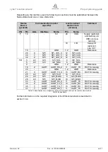
Page 33: ...PI_nCS 32 Z SPI SPI_nCS_Z 12 SPI_nCS 10 3 All I2C I2C_SCL 4 I2C_SCL 5 All I2C I2C_SDA 6 I2C_SDA 9 GND 1 2 GND Reference 18 Z UART UART_RX_Z 11 UART_TX RX TX crossing 20 GND 1 2 GND Reference 21 X UART...

Page 34: ...e communication interfaces as schematically illustrated in figure 1 21 The special features of the interface are explained in the sections 3 4 3 1 3 4 3 3 Integration of the Wittenstein communication...

Page 35: ...stein software stack with ADCS without any problems For synchronous setpoint transmission please observe the information in the introduction of this chapter 3 4 3 2 SPI interface The SPI bus is a mast...

Page 36: ...et the UART switching selection switch see figure 1 8 to UART uC As UART is a point to point connection a separate UART channel must be provided for each cyber reaction wheel 2 Alternatively a multipl...

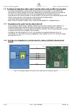
Page 37: ...tionwheel 3 5 Diagnostics using the cyber reaction wheel assistant In the case of a prototypical integration of the reaction wheel see section 3 4 parallel diagnostics with the cyber reaction wheel as...

Page 38: ...elp For this purpose open the cyber reaction wheel assistant open the CHM Help by pressing F1 enter firmware update in the search screen Notice During the firmware update the I2C address is reset to t...

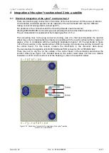
Page 39: ...lug connector routing vias etc that accommodates the reaction wheel may only be implemented as closely as possible with the reaction wheel within a radius of approx 2 mm in compliance with the constra...

Page 40: ...st have a diameter of 2 6 mm A position tolerance of 0 2 mm for compensation of any position and length deviations of the connectors must be observed 4 3 Installation of the cyber reaction wheel 2 Obs...

Page 41: ...tance of 1 mm on all sides of the drive system must be observed 4 6 Mounting position Any mounting position can be selected 4 7 Cooling Sufficient thermal conduction for cooling of the drive system mu...

Reviews: