7
Circuit description
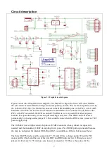
Figure 2 : Wisp648 circuit diagram
Figure 2 shows the Wisp648 circuit diagram. The MAX232 chip in the lower left corner handles
the conversion between RS232 voltage levels and polarity, and the TTL levels and polarity used by
the 16F648A PIC chip. The MAX232 connects to the RB1 and RB2 pins of the PIC, so the UART
hardware of the PIC can be used. The LED (above the MAX232) is connected to pin RA4 of the
PIC, so the PIC can switch the LED on and off. Pin RA4 is not very useful for other purposes
because it is open-drain only (it can not pull itself high, only low). The LED can be activated
permanently by closing solder jumper J2. This could be done when the PCB is (mis-) used as 7805
power supply only.
The 16F648A (lower right corner) chip has a 20 MHz resonator (cheap, robust, no capacitors
needed) and the mandatory 100nF decoupling for its power. No MCLR pull-up is needed because
the chip is configured for internal MCLR (pin RA5 is available as I/O pin, but not used here).
The three BAT85 diodes and the capacitors C7, C8 and C9 are a charge pump. When the PIC
makes pin RA2 high, and then switches pins RB3 and RB0 high and low (180 degrees out of
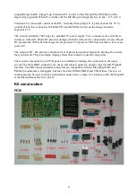
phase) it will create 3 x 5V (minus some losses) on capacitor C9. This is the source for the


