NINA-B3 series - System integration manual
UBX-17056748 - R13
System description
Page 9 of 72
C1-Public
1.3
Pin configuration and function
See the NINA-B3 series data sheet
for information about pin configuration and function.
1.4
Supply interfaces
1.4.1
Main supply input
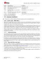
The NINA-B3 series uses an integrated DC/DC converter to transform the supply voltage presented
at the
VCC
pin into a stable system core voltage. Because of this, the NINA-B3 modules are
compatible for use in battery powered designs.
When using the NINA-B3 with a battery, it is important that the battery type can handle the peak
power of the module. For the battery supply, consider adding extra capacitance on the supply line to
avoid capacity degradation. See the NINA-B3 series data sheet
supply requirements and current consumption.
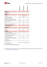
Table 2: Summary of voltage supply requirements
☞
The current requirement in
considers using the u-connectXpress software with UART
communications. But it does not include any additional I/O current. Any use of external push
buttons, LEDs, or other interfaces will add to the total current consumption of the NINA-B3
module. The peak current consumption of the entire design will need to be taken into account
when considering a battery powered solution.
1.4.2
Digital I/O interfaces reference voltage (VCC_IO)
On NINA-B3 series modules, the I/O voltage level is the same as the supply voltage and
VCC_IO
is
internally connected to the supply input
VCC
.
When using NINA-B3 with a battery, the I/O voltage level will vary with the battery output voltage,
depending on the charge of the battery. Level shifters might be needed depending on the I/O voltage
of the host system.
1.4.3
VCC application circuits
The power for NINA-B3 series modules is provided through the VCC pins, which can be one of the
following:
•
Switching Mode Power Supply (SMPS)
•
Low Drop Out (LDO) regulator
•
Battery
The SMPS is the ideal choice when the available primary supply source has a higher value than the
operating supply voltage of the NINA-B3 series modules. The use of SMPS provides the best power
efficiency for the overall application and minimizes the current drawn from the main supply source.
⚠
While selecting SMPS, ensure that the AC voltage ripple at the switching frequency is kept as low
as possible. Layout shall be implemented to minimize impact of high frequency ringing.
The use of an LDO linear regulator is convenient for a primary supply with a relatively low voltage
where the typical 85-90% efficiency of the switching regulator leads to minimal current saving. Linear
regulators are not recommended for high voltage step-down, as these dissipate a considerable
amount of energy.
Rail
Voltage requirement
Current requirement (peak)
VCC
1.7 V
–
3.6 V
20 mA
VCC_IO
Tied to VCC


