NINA-B3 series - System integration manual
UBX-17056748 - R13
Appendix
Page 68 of 72
C1-Public
B.1.1
Floor plan
This section describes where the critical components and copper traces are positioned on the
reference design.
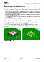
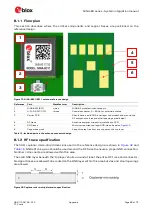
Figure 31: NINA-B301/B311 antenna reference design
Reference
Part
Manufacturer
Description
1
NINA-B301/B311
u-blox
NINA-B3 module with antenna pin
2
U.FL-R-SMT-1(10)
Hirose
Coaxial connector, 0
–
6 GHz, for external antenna
3
Carrier PCB
Should have a solid GND inner layer underneath and around the
RF components (vias and small openings are allowed)
4
RF trace
Antenna coplanar microstrip, matched to 50
Ω
5
GND trace
Minimum required top layer GND-trace. See also
6
Copper keep-out
Keep this area free from any copper on the top layer
Table 15: Included parts in the antenna connector design
B.1.2
RF trace specification
The 50
Ω
coplanar micro-strip dimensions used in the reference design are shown in
. GND stitching vias should be used around the RF trace to ensure a proper GND connection.
No other components are allowed within this area.
The solid GND layer beneath the ‘top layer’ shall surround at l
east the entire RF trace and connector.
No signal traces are allowed to be routed on the GND layer within this area but vias and small openings
are allowed.
Figure 32: Coplanar micro-strip dimension specification
1
2
3
4
5
6

