NINA-B3 series - System integration manual
UBX-17056748 - R13
Design-in
Page 40 of 72
C1-Public
There is no strict requirement for adding bypass capacitance to the supply net close to the module.
But depending on the layout of the supply net and other consumers on the same net, bypass
capacitors might still be beneficial. Though the GND pins are internally connected, connect all the
available pins to solid ground on the application board, as a good (low impedance) connection to an
external ground can minimize power loss and improve RF and thermal performance.
3.5
Serial interfaces
3.5.1
Asynchronous serial interface (UART) design
The layout of the UART bus should be made so that noise injection and cross talk are avoided.
It is recommended to use the hardware flow control with RTS/CTS to prevent temporary UART buffer
overrun.
The flow control signals RTS/CTS are active low thus a 0 (ON state =low level) will allow the UART to
transmit.
•
CTS is an input to the NINA-B3 module. If the host applies a 0 (ON state = low level) the module is
allowed to transmit.
•
RTS is an output off the NINA-B3 module. The module applies a 0 (ON state = low level) when it is
ready to receive transmission.
3.5.2
Serial peripheral interface (SPI)
The layout of the SPI bus should be made so that noise injection and cross talk are avoided.
3.5.3
I2C interface
The layout of the I2C bus should be made so that noise injection and cross talk are avoided.
3.5.4
QSPI interface
The layout of the QSPI bus should be made so that noise injection and cross talk are avoided.
3.5.5
USB interface
The layout of the USB bus should be made so that noise injection and cross talk are avoided.
3.6
NFC interface
⚠
The pins for the NFC interface can also be used as normal GPIOs. In NINA-B30 series modules,
ensure that the NFC pins are configured correctly in software. Connecting an NFC antenna to the
pins configured as GPIO will damage the module. In NINA-B31 series modules, the NFC pins will
always be set to "NFC mode".
The NFC antenna coil must be connected differentially between the
NFC1
and
NFC2
pins of the
device.
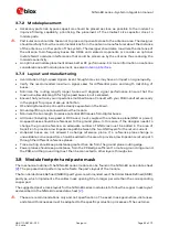
Two external capacitors should be used to tune the resonance of the antenna circuit to 13.56 MHz.
The required tuning capacitor value is given by the below equations: an antenna inductance of L
ANT
=
2
μ
H will give tuning capacitors in the range of 130 pF on each pin. For good performance, match the
total capacitance on NFC1 and NFC2.


