LEXI-R422 - System integration manual
UBX-23007449 - R02
Design-in
Page 78 of 108
C1-Public
2.6.3
I2C interface
2.6.3.1
Guidelines for I2C circuit design
The I2C-bus host interface can be used to communicate with u-blox GNSS receivers and other
external I2C-bus devices.
The
SDA
and
SCL
pins of the module are open drain output as per I2C bus specifications
, and they
have internal pull-up resistors to the
V_INT
1.8 V supply rail of the module, so there is no need of
additional pull-up resistors on the external application board.
☞
Capacitance and series resistance must be limited on the bus to match the I2C specifications
(maximum proper rise time for
SCL
/
SDA
lines is 1.0 µs): route connections as short as possible.
☞
ESD sensitivity rating of the I2C pins is 1 kV (HBM according to JS-001-2017). Higher protection
level could be required if the lines are externally accessible and it can be achieved by mounting an
ESD protection (e.g. EPCOS CA05P4S14THSG varistor) close to accessible points.
☞
If the pins are not used as I2C bus interface, they can be left unconnected.
Connection with u-blox 1.8 V GNSS receivers
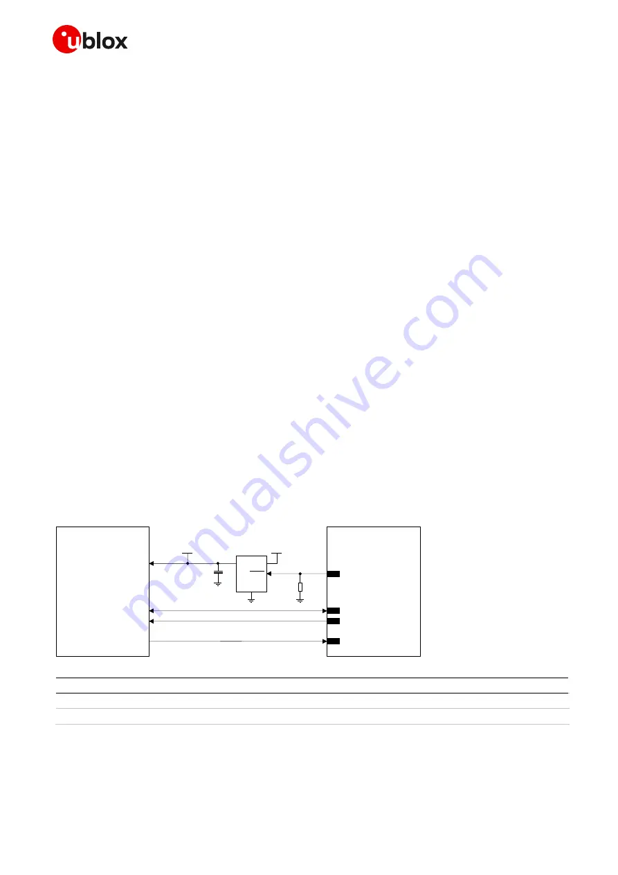
shows an application circuit for connecting the cellular module to an external u-blox 1.8 V
GNSS receiver:
•
The
SDA
and
SCL
pins of the cellular module are directly connected to the related pins of the u-blox
1.8 V GNSS receiver. External pull-up resistors are not needed, as they are already integrated in
the cellular module.
•
The
GPIO2
pin is connected to the active-high enable pin of the voltage regulator that supplies the
u-blox 1.8 V GNSS receiver pro
viding the “GNSS supply enable” function. A pull
-down resistor is
provided to avoid a switch on of the positioning receiver when the cellular module is switched off
or in the reset state.
•
The
GPIO3
pin is connected to the
TxD
pin of the u-blox 1.8 V GNSS receiver providing the
additional “GNSS Tx data ready” function.
IN
OUT
GND
GNSS LDO
regulator
SHDN
u-blox GNSS
1.8 V receiver
SDA
SCL
VMAIN
1V8
U1
R3
GPIO2
SDA
SCL
C1
P1
N1
VCC
R1
GNSS supply enable
LEXI-R422
TxD
GPIO3
R4
GNSS data ready
Figure 59: Application circuit for connecting LEXI-R422 modules to u-blox 1.8 V GNSS receivers
Reference
Description
Part number - Manufacturer
R1
47 k
Ω
resistor 0402 5% 0.1 W
RC0402JR-0747KL - Yageo Phycomp
U1
Voltage regulator for GNSS receiver
See GNSS receiver hardware integration manual
Table 36: Components for connecting LEXI-R422 modules to u-blox 1.8 V GNSS receivers
☞
For additional guidelines regarding the design of applications with u-blox 1.8 V GNSS receivers,
see the hardware integration manual of the u-blox GNSS receivers.
☞
For additional guidelines regarding cellular and GNSS RF coexistence, see section


