


THCV242_ Rev.2.00_E
Copyright
©
2019 THine Electronics, Inc. THine Electronics, Inc.
35/53
Security E
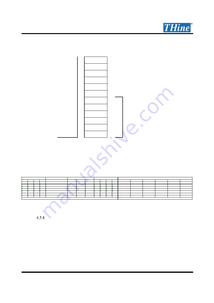
MTX0P/N and MTX2P/N can be assigned to be MIPI 2nd port (port1).
Figure 13.
MIPI 2nd port available pins
Setting of MIPI 2port output examples are shown below.
Table 22.
MIPI 2port output setting example
MIPI CSI-2 Virtual Channel
MIPI Virtual Channel (VC) is supported. When MIPI PH(Packet Header) is intake from V-by-One® HS input,
MIPI Virtual Channel information in PH is also bridged from V-by-One® HS at the same time. Virtual Channel
information can be intake from Main-Link input and properly applied on MIPI Packet Header by selectable
register setting.
28
MTX3P
27
MTX3N
26
MTX1P
25
MTX1N
24 MTXCLK0P
23 MTXCLK0N
22
MTX0P
MIPI Tx
21
MTX0N
available
20
MTX2P
2nd port1
19
MTX2N
data pins
18 MTXCLK1P
2nd port1 clock
17 MTXCLK1N
2nd port1 clock
THCV242
R_TX_LANE_SEL1
lane3
lane2
lane1
lane0
port1 select
port enable clk enable
config
lane3
lane2
lane1
lane0
lane3
lane1
lane0
lane2
[7:6]
[5:4]
[3:2]
[1:0]
[1:0]
[6:5]
[4:3]
[2:0]
[3]
[2]
[1]
[0]
MTX3P/N
MTX1P/N
MTXCLK0P/N
MTX0P/N
MTX2P/N
MTXCLK1P/N
01
11
00
10
00
11
11
101
0
1
0
1
port0 2nd Byte
port0 1st Byte
port0 clock
port1 1st Byte
port1 2nd Byte
port1 clock
01
10
00
11
10
11
11
101
0
1
0
1
port0 2nd Byte
port0 1st Byte
port0 clock
port1 2nd Byte
port1 1st Byte
port1 clock
00
11
01
10
00
11
11
101
0
1
0
1
port0 1st Byte
port0 2nd Byte
port0 clock
port1 1st Byte
port1 2nd Byte
port1 clock
01
11
00
10
00
11
11
100
0
1
0
1
No output
port0 1st Byte
port0 clock
port1 1st Byte
No output
port1 clock
01
10
00
11
10
11
11
100
0
1
0
1
No output
port0 1st Byte
port0 clock
No output
port1 1st Byte
port1 clock
00
11
01
10
00
11
11
100
0
1
0
1
port0 1st Byte
No output
port0 clock
port1 1st Byte
No output
port1 clock
R_TX_LANE_SEL0
R_LANE_EN
R_REQ_SEL
MIPI Physical pin order output assignment
other settings
forbidden