L M K 0 4 9 0 6 E V A L U A T I O N B O A R D O P E R A T I N G I N S T R U C T I O N S
SNAU126
22
by the reference input of PLL2 now. The PLL2 reference frequency will remain at the VCXO
frequency.
When the PLL1 VCXO frequency is different from the PLL2 reference frequency, a warning
will be displayed on the clock outputs tab informing the user that PLL1 VCO and PLL2
reference frequency are mismatched and the one or more of the PLLs are out of lock. While
there still could be an error in the divider values which may cause a non-locked PLL, this
warning by itself may no longer be assumed true. It is up to the user to ensure the PLL dividers
are programmed correctly.
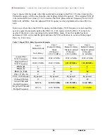
To illustrate the proper programming of the LMK04906 device in dual loop 0-delay mode the
following case examples are provided. Note that in one of the cases, the feedback frequency
from the clock output matches the VCXO frequency and CodeLoader will display the proper
frequency values.
Dual Loop 0-Delay (MODE=2 or 5) Case 1: For example the default configuration, 122.88 MHz
CLKin, 122.88 MHz VCXO, of the LMK04906 has the following register programming.
Case 1:
Default Mode
No 0-Delay
Case2:
Default 0-Delay
Mode
(CLKout4 =
122.88 MHz)
Case 3:
Default 0-Delay
Mode (Updated
CLKout4 =
245.76 MHz)
Case 4:
Default 0-Delay
Mode (Updated
CLKout4 =
61.44 MHz)
Actual PLL1
VCXO Frequency
122.88
122.88
122.88
122.88
Reported PLL1
VCXO Frequency
122.88
122.88
61.44
245.76
PLL1 N
120
120
60
240
Actual PLL2
VCO Frequency
2949.12 MHz
2949.12 MHz
2949.12 MHz
2949.12 MHz
Reported PLL2
VCO Frequency
2949.12 MHz
2949.12 MHz
2949.12 MHz
2949.12 MHz
PLL2_N
12
12
12
12
PLL2_P (Pre-N)
2
2
2
2
PLL2 VCO Divider
Bypassed
Bypassed
Bypassed
Bypassed
CLKout8 Divide
12
24
12
48
Actual CLKout8
Output Frequency
245.76 MHz
122.88 MHz
245.76 MHz
61.44 MHz
Reported CLKotu8
Output Frequency
245.76 MHz
122.88 MHz
245.76 MHz
61.44 MHz


