background image


L M K 0 4 9 0 6   E V A L U A T I O N   B O A R D   O P E R A T I N G   I N S T R U C T I O N S  


SNAU126 

21 

Programming 0-Delay Mode in CodeLoader 

Overview 

When enabling the 0-Delay mode the feedback path of the VCO is altered to include a clock 
output.  See the datasheet for more details on 0-Delay functionality. 
 
The current version of the CodeLoader software does not include this extra divider in the 
frequency calculations when in holdover mode.  To successfully lock the LMK04906 device in a 
0-Delay mode the user must program the device “manually” account for this divider.  
Programming “manually” means that the VCO frequency and therefore the clock output 
frequencies displayed by the CodeLoader software may be incorrect.  For the LMK04906 device 
to lock properly the 

divider values

 must be programmed correctly.  The frequencies displayed in 

the application are only for the benefit of the user and for proper automatic programming of the 
OSCin_FREQ register which will not be affected by 0-Delay. 
 
When using the device in Dual Loop mode vs. Single Loop mode different procedures are used 
to cause the device to lock when using the CodeLoader software.  The following two sections 
describe the process for when the LMK04906 device is programmed for a Dual Loop mode and 
Single Loop mode respectively.  Each section contains a brief introduction, the programming 
steps to execute to make the device lock, and finally a detailed section discussing the 
workaround and some example cases. 
  

Dual Loop 0-Delay Mode Examples 

In Dual Loop 0-Delay Modes, MODE = 2 or MODE = 5, the feedback from the VCXO of PLL1 
to the PLL1 N divider is broken and a clock output will drive the PLL1 N divider.  This permits 
phase alignment between the clock output and the clock input (0-Delay).  As such, the PLL1_N 
and PLL1_R divide values may need to be adjusted to permit the LMK04906 to lock. 

Programming Steps 

1.


Program a Dual Loop 0-Delay mode. 

2.


Enable the feedback mux.  EN_FEEDBACK_MUX = 1. 

3.


Select clock output for feedback with the feedback mux.  FEEDBACK_MUX = User 
value. 

4.


Program the VCXO (VCO) frequency of PLL1 tab to the clock output frequency selected 
by the feedback mux. 

 
If for any reason the CLKout frequency is less than the phase detector frequency, the PLL1 R 
divider must be increased so that the phase detector is at the same or lower value than the 
CLKout frequency. 

Details 

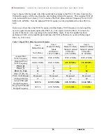
When using the CodeLoader software in Dual Loop 0-Delay mode, programming the VCXO 
(VCO) frequency of the PLL1 tab to the frequency of the fed back output clock will re-program 
the PLL1 N divider to allow the LMK04906 will be able to lock.  The PLL1 loop has been 
altered and actual VCXO no longer directly feeds into PLL1 N divider.  The VCXO is only used 

Summary of Contents for LMK04906B

Page 1: ...A L U A T I O N B O A R D O P E R A T I N G I N S T R U C T I O N S SNAU126 1 LMK04906 Family Low Noise Clock Jitter Cleaner with Dual Loop PLLs LMK04906 Evaluation Board Operating Instructions Texas Instruments June 2012 ...

Page 2: ...UTPUTS 9 PLL LOOP FILTERS AND LOOP PARAMETERS 11 PLL 1 LOOP FILTER 11 122 88 MHz VCXO PLL 11 PLL2 LOOP FILTER 12 EVALUATION BOARD INPUTS AND OUTPUTS 13 RECOMMENDED TEST EQUIPMENT 20 PROGRAMMING 0 DELAY MODE IN CODELOADER 21 OVERVIEW 21 DUAL LOOP 0 DELAY MODE EXAMPLES 21 Programming Steps 21 Details 21 SINGLE LOOP 0 DELAY MODE EXAMPLES 23 Programming Steps 23 Details 23 APPENDIX A CODELOADER USAGE ...

Page 3: ...WIRE HEADER LOGIC I O PORTS AND STATUS LEDS 46 APPENDIX D BILL OF MATERIALS 47 APPENDIX E PCB LAYERS STACKUP 52 APPENDIX F PCB LAYOUT 53 LAYER 1 TOP 53 LAYER 2 RF GROUND PLANE INVERTED 54 LAYER 3 VCC PLANES 55 LAYER 4 GROUND PLANE INVERTED 56 LAYER 5 VCC PLANES 2 57 LAYER 6 BOTTOM 58 LAYERS 1 AND 6 TOP AND BOTTOM COMPOSITE 59 APPENDIX G PROPERLY CONFIGURING LPT PORT 60 LPT DRIVER LOADING 60 CORREC...

Page 4: ...e 1 1 CodeLoader uWire cable LPT uWire Available LMK04906 Evaluation Boards The LMK04906 Evaluation Board supports any of the four devices offered in the LMK04906 Family All evaluation boards use the same PCB layout and bill of materials except for the corresponding LMK04906B device affixed to the board A commercial quality VCXO is also mounted to the board to provide a known reference point for e...

Page 5: ...IRE IFACE at www ti com 4 Program the device with a default mode using CodeLoader Ctrl L must be pressed at least once to load all registers Alternatively click menu Keyboard Controls Load Device CodeLoader can be downloaded from www ti com tool codeloader 5 Measurements may be made on an active output clock port via its SMA connector CLKout0 CLKout0 Laptop or PC Parallel Port Connector 5 0 V LDO ...

Page 6: ...re to enable the output under test to make measurements Table 3 Default CodeLoader Modes for LMK04906 Default CodeLoader Mode Device Mode CLKin Frequency OSCin Frequency 122 88 MHz CLKin1 122 88 MHz VCXO Dual PLL Internal VCO 122 88 MHz 122 88 MHz 122 88 MHz CLKin1 Dual Loop 0 delay 122 88 MHz VCXO Dual PLL Internal VCO 0 Delay with Internal Feedback 122 88 MHz 122 88 MHz 122 88 MHz CLKin1 122 88 ...

Page 7: ...r Before proceeding be sure to follow the Quick Start section above to ensure proper connections 1 Start CodeLoader 4 Application Click Start Programs CodeLoader 4 CodeLoader 4 The CodeLoader 4 program is installed by default to the CodeLoader 4 application group 2 Select Device Click Select Device Clock Conditioners LMK04906B Once started CodeLoader 4 will load the last used device To load a new ...

Page 8: ...sn t really needed but included to emphasize the importance of pressing Ctrl L to load the device at least once after starting CodeLoader restoring a mode or restoring a saved setup using the File menu See Appendix A CodeLoader Usage or the CodeLoader 4 instructions located at http www ti com tool codeloader for more information on Port Setup Appendix H Troubleshooting Information contains informa...

Page 9: ...a Digital Delay value b Clock Divider value c Analog Delay select and Analog Delay value if not Bypassed d Clock Output type 4 Depending on the configured output type the clock output SMAs can be interfaced to a test instrument with a single ended 50 ohm input as follows a For LVDS i A balun like ADT2 1T is recommended for differential to single ended conversion b For LVPECL i A balun can be used ...

Page 10: ... The phase noise may be measured with a spectrum analyzer or signal source analyzer See Appendix B Typical Phase Noise Performance Plots for phase noise plots of the clock outputs TI s Clock Design Tool can be used to calculate divider values to achieve desired clock output frequencies See http www ti com tool codeloader ...

Page 11: ...gured for a narrow loop bandwidth 100 Hz while the loop filter of PLL2 has been configured for a wide loop bandwidth 100 kHz The specific loop bandwidth values depend on the phase noise performance of the oscillator mounted on the board The following tables contain the parameters for PLL1 and PLL2 for each oscillator option TI s Clock Design Tool can be used to optimize PLL phase noise jitter for ...

Page 12: ... 047 nF C2_A2 3 9 nF C3 internal 0 nF C4 internal 0 nF R2_A2 0 62 kΩ R3 internal 0 2 kΩ R4 internal 0 2 kΩ Charge Pump Current K 3 2 mA Phase Detector Frequency 122 88 MHz Frequency 2457 6 MHz Kvco 18 8 MHz V N 20 Phase Margin 75 degrees Loop Bandwidth 321 kHz Note PLL Loop Bandwidth is a function of K Kvco N as well as loop components Changing K and N will change the loop bandwidth ...

Page 13: ...ut3 CLKout3 CLKout4 CLKout4 CLKout5 CLKout5 Analog Output Clock outputs with programmable output buffers The output terminations by default on the evaluation board are shown below and the output type selected by default in CodeLoader is indicated by an asterisk Clock output pair Default Board Termination CLKout0 LVPECL CLKout1 LVPECL CLKout2 LVDS LVCMOS CLKout3 LVDS LVCMOS CLKout4 LVDS LVCMOS CLKo...

Page 14: ...e evaluation board A 3 9 V DC power source applied to this SMA will by default source the onboard LDO regulators that power the inner layer planes that supply the LMK04906B and its auxiliary circuits e g VCXO The LMK04906B contains internal voltage regulators for the VCO PLL and other internal blocks The clock outputs do not have an internal regulator so a clean power supply with sufficient output...

Page 15: ...elected in CodeLoader The clock input selection mode can be programmed on the Bits Pins tab via the CLKin_Select_MODE control Refer to the LMK04906 Family Datasheet section Input Clock Switching for more information AC coupled Input Clock Swing Levels Input Mode Min Max Units Differential Bipolar or CMOS 0 5 3 1 Vpp Single Ended 0 25 2 4 Vpp External Feedback Input FBCLKin for 0 Delay CLKin1 is sh...

Page 16: ...VCXO device A single ended or differential signal may be used to drive the OSCin OSCin pins and must be AC coupled If operated in single ended mode the unused input must be connected to GND with 0 1 uF Refer to the LMK04906 Family Datasheet section Electrical Characteristics for PLL2 Reference Input OSCin specifications Test point VTUNE1_TP Analog Output Tuning voltage output from the loop filter ...

Page 17: ...ection Status Pins and Digital Lock Detect for more information Note Before a high frequency internal signal e g PLL divider output signal is selected by LD_MUX it is suggested to first remove the 270 ohm resistor to prevent the LED from loading the output Test point Holdover_TP CMOS Output Programmable status output pin By default set to the output holdover mode status signal In the default CodeL...

Page 18: ... Mode When CLKin_SELECT_MODE is 3 the Status_CLKinX pins select which clock input is active as follows Status_CLKin1 Status_CLKin0 Active Clock 0 0 CLKin0 0 1 CLKin1 1 0 CLKin2 1 1 Holdover Input Clock Switching Auto with Pin Select When CLKin_SELECT_MODE is 6 the active clock is selected using the Status_CLKinX pins upon an input clock switch event as follows Status_CLKin1 Status_CLKin0 Active Cl...

Page 19: ...e SYNC will asserted when the SYNC pin is low and the outputs to be synchronized will be held in a logic low state When SYNC is unasserted the clock outputs to be synchronized are activated and will be initially phase aligned with each other except for outputs programmed with different digital delay values A SYNC event can also be programmed by toggling the SYNC_POL_INV bit in the Bits Pins tab in...

Page 20: ...or for phase noise measurements At frequencies less than 100 MHz the local oscillator noise of the E4445A is too high and measurements will reflect the E4445A s internal local oscillator performance not the device under test Oscilloscope To measure the output clocks for AC performance such as rise time or fall time propagation delay or skew it is suggested to use a real time oscilloscope with at l...

Page 21: ...l Loop mode and Single Loop mode respectively Each section contains a brief introduction the programming steps to execute to make the device lock and finally a detailed section discussing the workaround and some example cases Dual Loop 0 Delay Mode Examples In Dual Loop 0 Delay Modes MODE 2 or MODE 5 the feedback from the VCXO of PLL1 to the PLL1 N divider is broken and a clock output will drive t...

Page 22: ...e feedback frequency from the clock output matches the VCXO frequency and CodeLoader will display the proper frequency values Dual Loop 0 Delay MODE 2 or 5 Case 1 For example the default configuration 122 88 MHz CLKin 122 88 MHz VCXO of the LMK04906 has the following register programming Case 1 Default Mode No 0 Delay Case2 Default 0 Delay Mode CLKout4 122 88 MHz Case 3 Default 0 Delay Mode Update...

Page 23: ...is programmed PLL2_N_CAL value is automatically updated when a new VCO frequency is entered and the PLL2_N value is calculated In this case the VCO frequency entered is wrong and the PLL2_N_CAL value will be incorrect If for any reason the CLKout frequency is less than the phase detector frequency the PLL2 R divider must be increased so that the phase detector is at the same or lower value than th...

Page 24: ...vice were operating in the non 0 Delay mode Once this update has been performed Ctrl L will reload the part and cause the VCO calibration to occur with the proper PLL2_N_CAL value Table 7 Single PLL 0 Delay Operation Examples Case 1 Default Mode No 0 Delay Case 2 Default 0 Delay Mode CLKout4 1474 56 MHz Case 3 Default 0 Delay Mode Updated CLKout4 245 76 MHz Case 4 Default 0 Delay Mode Updated CLKo...

Page 25: ...ble from http www ti com tool usb2uwire iface The part number is USB2UWIRE IFACE Port Setup Tab Figure 8 Port Setup tab On the Port Setup tab the user may select the type of communication port USB or Parallel that will be used to program the device on the evaluation board If parallel port is selected the user should ensure that the correct port address is entered The Pin Configuration field is har...

Page 26: ...a OSC Mux1 and OSC Mux2 Channel Powerdown affects digital and analog delay clock divider and buffer blocks Digital Delay value and Half Step Clock Divide value Analog Delay value and Delay bypass enable per output Clock Output format per output This tab also allows the user to select the VCO Divider value 2 to 8 Note that the total PLL2 N divider value is the product of the VCO Divider value and t...

Page 27: ...gh the possible values Left click to increase the component value and right click to decrease the value These values can also be changed in the Bits Pins tab The Reference Oscillator value field may be changed in either the Clock Outputs tab or the PLL2 tab The PLL2 Reference frequency should match the frequency of the onboard VCXO or Crystal i e VCO frequency in the PLL1 tab if not a warning mess...

Page 28: ... 8 Table 8 Registers Controls and Descriptions in PLL1 tab Control Name Register Name Description Reference Oscillator Frequency MHz n a CLKin frequency of the selected reference clock Phase Detector Frequency MHz n a PLL1 Phase Detector Frequency PDF This value is calculated as PLL1 PDF CLKin Frequency PLL1_R CLKinX_PreR_DIV where CLKinX_PreR_DIV is the predivider value of the selected input cloc...

Page 29: ...e Frequency When operating in Dual PLL mode without 0 delay feedback the VCO frequency value on the PLL1 tab must match the Reference Oscillator OSCin frequency value on the PLL2 tab otherwise the one or both PLLs may be out of lock Updating the Reference Oscillator frequency on the PLL2 tab will automatically update the value of OSCin_FREQ on the Bits Pins tab However when operating in Dual PLL m...

Page 30: ...ernal VCXO or Crystal Phase Detector Frequency MHz n s PLL2 Phase Detector Frequency PDF This value is calculated as PLL2 PDF OSCin Frequency 2EN_PLL2_REF_2X PLL2_R VCO Frequency MHz n a Internal VCO Frequency should be within the allowable range of the LMK04906B device This value is calculated as VCO Frequency PLL2 PDF PLL2_N PLL2_P VCO divider value Doubler EN_PLL2_REF_2X PLL2 Doubler 0 Bypass D...

Page 31: ...es made on this tab will be reflected in the Clock Outputs tab The VCO Frequency should conform to the specified internal VCO frequency range for the LMK04906B device per Table 2 Bits Pins Tab Figure 13 Bits Pins tab The Bits Pins tab allows the user to program bits directly many of which are not available on other tabs Brief descriptions for the controls on this tab are provided in Table 10 to su...

Page 32: ...istribution path The VCO divider is only valid if MODE is selecting the Internal VCO uWire_LOCK When checked no other uWire programming will have effect Must be unchecked to enable uWire programming of registers R0 to R30 CLKin CLKin_Select_MODE Selects operational mode for how the device selects the reference clock for PLL1 EN_CLKin1 Enables CLKin1 as a usable reference input during auto switchin...

Page 33: ...t and Y odd numbered output SYNC_QUAL Sets the SYNC to qualify mode for dynamic digital delay EN_SYNC Must be set when using SYNC but may be cleared after the SYNC event When using dynamic digital delay SYNC_QUAL 1 EN_SYNC must always be set Changing this value from 0 to 1 can cause a SYNC event so clocks which should not be SYNCed when setting this bit should have the NO_SYNC_CLKoutX_Y bit set NO...

Page 34: ...DAC_HIGH_TRIP Value from VCC 3 3V in 50mV steps at which clock switch event is generated If Holdover mode is enabled it will be engaged upon the clock switch event NOTE EN_VTUNE_RAIL_DET must be enabled for this to be valid PLL1 PLL1_WND_SIZE If the phase error between the PLL1 reference and feedback clocks is less than specified time then the PLL1 lock counter increments NOTE Final lock detect va...

Page 35: ..._PLL2_REF_2X Enables the doubler block to doubles the reference frequency into the PLL2 R counter This can allow for frequency of 2 3 2 5 etc of OSCin to be used at the phase detector of PLL2 PLL2_N_CAL The PLL2_N_CAL register contains the N value used for the VCO calibration routine Except during 0 delay modes the PLL2_N and PLL2_N_CAL registers will be exactly the same PLL2_R3_LF Set the corresp...

Page 36: ...ters Tab The Registers tab shows the value of each register This is convenient for programming the device to the desired settings then exporting to a text file the register values in hexadecimal for use in your own application By clicking in the bit field it is possible to manually change the value of registers by typing 1 and 0 ...

Page 37: ...k phase noise measurements with the Crystek 122 88 MHz VCXO Table 11 LMK04906B Test Conditions Parameter Value PLL1 Reference clock input CLKin0 single ended input CLKin0 AC coupled to GND PLL1 Reference Clock frequency 122 88 MHz PLL1 Phase detector frequency 122 88 MHz PLL1 Charge Pump Gain 100 uA VCXO frequency 122 88 MHz PLL2 phase detector frequency 122 88 MHz PLL2 Charge Pump Gain 3200 uA PL...

Page 38: ...34 5 1 MHz 32 9 10 MHz 22 7 Clock Output Measurement Technique The same technique was used to measure phase noise for all three output types available on the programmable OSCout and CLKout buffers This was achieved by terminating one side of the LVPECL LVDS or LVCMOS output with a 50 ohm load and measuring the other side single ended using an Agilent E5052B Source Signal Analyzer Buffered OSCout P...

Page 39: ...Noise Figure 16 LMK04906B CLKout Phase Noise Table 14 LMK04906B Phase Noise dBc Hz Phase Noise and RMS Jitter fs Offset 1474 56 MHz LVDS 1474 56 MHz LVPECL 491 52 MHz LVDS 491 52 MHz LVPECL 100 Hz 88 9 88 3 99 9 99 0 1 kHz 109 1 109 5 117 7 119 5 10 kHz 119 0 119 1 126 9 126 5 100 kHz 121 2 121 2 129 4 129 5 800 kHz 133 6 133 6 141 6 141 7 1 MHz 135 4 135 5 143 5 143 6 10 MHz 149 9 151 0 154 2 156...

Page 40: ...fset 245 76 LVDS 245 76 LVPECL 245 76 LVCMOS 122 88 LVDS 122 88 LVCMOS 122 88 LVPECL 100 Hz 106 2 103 4 102 9 110 3 110 5 108 1 1 kHz 124 8 124 0 124 1 130 2 130 2 130 8 10 kHz 133 0 132 7 133 7 139 2 137 4 139 1 100 kHz 135 6 135 6 135 7 141 8 141 7 141 8 800 kHz 147 8 147 8 148 3 152 9 153 4 153 4 1 MHz 149 1 149 5 149 2 154 5 155 1 155 0 10 MHz 156 9 159 0 158 0 158 5 161 5 161 4 20 MHz 157 0 1...

Page 41: ...SCout Phase Noise Table 16 LMK04906B OSCout Phase Noise and RMS Jitter fs Offset OSCout0 LVPECL OSCin thru CLKout 100 Hz 106 8 104 7 1 kHz 135 5 133 1 10 kHz 147 8 147 3 100 kHz 155 5 154 4 800 kHz 157 6 156 1 1 MHz 157 5 156 2 10 MHz 158 6 155 7 20 MHz 158 4 157 1 RMS Jitter fs 10 kHz to 20 MHz 103 6 121 3 RMS Jitter fs 100 Hz to 20 MHz 118 4 135 3 ...

Page 42: ...U5 LP3878SD ADJ LP3878 ADJ 3 3 V component values C340 4 7 uF R350 51 k C346 0 01 uF R356 866 C352 10 uF R351 2 00 k C341 2 2 nF 0 1µF C72 1µF C71 1µF C89 DNP 1µF C93 DNP 1 1 2 2 J1 TERMBLOCK_2 IN 6 OUT 1 GND 3 EN 4 NC 5 DAP 7 NC 2 U7 LP5900SD 3 3 GND C359 0 47 uF C360 0 47 uF R369 51 k Designators greater than and equal to 300 are placed on bottom of PCB LP3878SD ADJ LP5900SD 3 3 LP5900 Component...

Page 43: ... are placed on bottom of PCB 10µF C37 0 1µF C39 CLKout0_P CLKout0_N CLKout1_P CLKout1_N CLKout2_P CLKout2_N CLKin0_P CLKin0_N CLKin1_P CLKin1_N CLKin2_P CLKin2_N Status_Hold Status_LD Status_CLKin0 Status_CLKin1 CLKout5_N CLKout5_P CLKout4_N CLKout4_P CLKout3_N CLKout3_P SYNC 0 R35 DNP uWire_DATA uWire_CLK uWire_LE OSCout0_N OSCout0_P Vcc1_VCO Vcc2_CLKout_CG1 Vcc3_CLKout_CG2 Vcc4_Digital Vcc5_CLKi...

Page 44: ...ce Matching and Attenuation CLKin1 0 R2 270 R4 DNP 0 1µF C2 0 1µF C10 0 1µF C6 DNP 100 R5 0 1µF C1 0 R8 0 1µF C9 CLKin0 Impedance Matching and Attenuation 270 R11 DNP 0 1µF C11 DNP 0 1µF C25 0 1µF C28 270 R29 DNP 270 R33 DNP CLKin2 Impedance Matching and Attenuation Vcc_VCO 100pF C17 DNP 0 1µF C16 0 R15 DNP CLKin0_P CLKin0_N CLKin1_P CLKin1_N CLKin2_P CLKin2_N 0 1µF C27 0 1µF C24 0 R27 0 R31 270 R...

Page 45: ...otes 1 Designators greater than and equal to 300 are placed on bottom of PCB 0 1µF C47 0 1µF C50 CLKout0 0 1µF C59 0 1µF C60 OSCout0_N OSCout0_P OSCout0 OSCout0_1_P OSCout0_1_N CLKout0_P CLKout0_N OSCout0 SMA OSCout0 SMA CLKout1 SMA CLKout1 SMA CLKout0 SMA CLKout0 SMA Default LVDS AC coupled Default LVPECL AC coupled Default LVPECL AC coupled Default LVPECL AC coupled 0 1µF C48 CLKout0_1_P CLKout0...

Page 46: ...n http www ti com Contact http www national com support LMK049xx Evaluation Board Project Designed for Evaluation Customer 870600738 1 Assembly Variant 12 21 2011 Texas Instruments CopyrightYear Holdover_TP TESTPOINT 100pF C45 DNP 27k R65 100pF C46 DNP 0 R61 DNP uWire Header and Level Translation Lock Detect Status Holdover Status SYNC Level Translation CLKin Select 270 R47 DNP 1 2 3 4 5 6 7 8 9 1...

Page 47: ...5C106M8PACTU 1 7 C3_VCXO CAP CERM 100pF 50V 5 C0G NP0 0603 Kemet C0603C101J5GACTU 1 8 C4 CAP CERM 2200pF 50V 10 X7R 0603 Kemet C0603C222K5RACTU 1 9 C5 CAP CERM 82pF 50V 10 C0G NP0 0603 Kemet C0603C820K5GACTU 1 10 C9 C15 C25 C28 R13 R14 R16 R27 R31 R42 R43 R99 R101 R105 R120 R123 CAP CERM 0 1uF 16V 10 X7R 0603 CAP CERM 0 1uF 25V 5 X7R 0603 RES 0 ohm 5 0 1W 0603 Vishay Dale CRCW06030000Z0EA 16 11 C1...

Page 48: ... Opto Components Inc SML LX2832GC 1 22 J1 CONN TERM BLK PCB 5 08MM 2POS OR Weidmuller 1594540000 1 23 R1 R100 R102 R103 R104 R106 R109 R111 R115 R121 R124 FB 120 ohm 500 mA 0603 Ferrite Murata BLM18AG121SN1D 11 24 R2 R8 R19 RES 0 ohm 5 0 1W 0603 RES 18 ohm 5 0 1W 0603 Vishay Dale CRCW060318R0JNEA 3 25 R2_VCO RES 620 ohm 5 0 1W 0603 Vishay Dale CRCW0603620RJNEA 1 26 R2_VCXO RES 39k ohm 5 0 1W 0603 ...

Page 49: ...22 88 1 39 U5 Micropower 800mA Low Noise Ceramic Stable Adjustable Voltage Regulator for 1V to 5V Applications Texas Instruments LP3878SD ADJ 1 40 U7 Ultra Low Noise 150mA Linear Regulator for RF Analog Circuits Requires No Bypass Capacitor Texas Instruments LP5900SD 3 3 1 41 uWire Low Profile Vertical Header 2x5 0 100 FCI 52601 G10 8LF 1 42 C2A_VCXO CAP CERM 2 7uF 10V 10 X5R 0805 Kemet C0805C275K...

Page 50: ... SMA 50 Ohm Emerson Network Power 142 0701 851 0 57 R3 R4 R10 R11 R28 R29 R32 R33 R46 R47 RES 270 ohm 5 0 1W 0603 Vishay Dale CRCW0603270RJNEA 0 58 R6 R7 RES 140 ohm 1 0 1W 0603 Vishay Dale CRCW0603140RFKEA 0 59 R9 R12 RES 8 2 ohm 5 0 1W 0603 Vishay Dale CRCW06038R20JNEA 0 60 R15 R22 R23 R24 R34 R35 R40 R41 R59 R61 R112 R113 R114 R116 R117 R119 R122 RES 0 ohm 5 0 1W 0603 Vishay Dale CRCW06030000Z0...

Page 51: ... N S T R U C T I O N S SNAU126 51 69 U4 Precison Single Low Noise Low 1 F corner Op Amp Texas Instruments LMP7731MF 0 70 U6 Ultra Low Noise 150mA Linear Regulator for RF Analog Circuits Requires No Bypass Capacitor Texas Instruments LP5900SD 3 3 0 71 Y300 DNP_XTAL 0 ...

Page 52: ...ils RF Ground plane 1 oz FR4 4 mils Power plane 1 1 oz FR4 12 6 mils Ground plane 1 oz FR4 8 mils Power Plane 2 1 oz FR4 12 mils Bottom Layer copper clad for thermal relief 2 oz RO4003 Er 3 3 16 mil Top Layer LMK049xxENG GTL RF Ground plane LMK049xxENG G1 FR4 Er 4 8 4 mil Power plane 1 LMK049xxENG G2 FR4 12 6 mil Ground plane LMK049xxENG GP1 FR4 12 mil Bottom Layer LMK049xxENG GBL 62 2 mil thick F...

Page 53: ...L M K 0 4 9 0 6 E V A L U A T I O N B O A R D O P E R A T I N G I N S T R U C T I O N S SNAU126 53 Appendix F PCB Layout Layer 1 Top ...

Page 54: ...L M K 0 4 9 0 6 E V A L U A T I O N B O A R D O P E R A T I N G I N S T R U C T I O N S SNAU126 54 Layer 2 RF Ground Plane Inverted ...

Page 55: ...L M K 0 4 9 0 6 E V A L U A T I O N B O A R D O P E R A T I N G I N S T R U C T I O N S SNAU126 55 Layer 3 Vcc Planes ...

Page 56: ...L M K 0 4 9 0 6 E V A L U A T I O N B O A R D O P E R A T I N G I N S T R U C T I O N S SNAU126 56 Layer 4 Ground Plane Inverted ...

Page 57: ...L M K 0 4 9 0 6 E V A L U A T I O N B O A R D O P E R A T I N G I N S T R U C T I O N S SNAU126 57 Layer 5 Vcc Planes 2 ...

Page 58: ...L M K 0 4 9 0 6 E V A L U A T I O N B O A R D O P E R A T I N G I N S T R U C T I O N S SNAU126 58 Layer 6 Bottom ...

Page 59: ...L M K 0 4 9 0 6 E V A L U A T I O N B O A R D O P E R A T I N G I N S T R U C T I O N S SNAU126 59 Layers 1 and 6 Top and Bottom Composite ...

Page 60: ...n improper mode The PC must be rebooted after install for LPT support to work properly Correct LPT Port Address To determine the correct LPT port in Windows open the device manager On Windows XP Start Settings Control Panel System Hardware tab Device Manager and check the LPT port under the Ports COM LPT node of the tree It can be helpful to confirm that the LPT port is mapped to the expected port...

Page 61: ... communications are not working then it is possible the LPT port mode is set improperly It is recommended to use the simple Output only mode of the LPT port This can be set in the BIOS of the computer Common terms for this desired parallel port mode are Normal Output or AT It is possible to enter BIOS setup during the initial boot up sequence of the computer ...

Page 62: ...LL1 i If not examine PLL1 register N programming ii If not examine physical OSCin input Naturally the output frequency of the above two items PLL 1 R Divider 2 and PLL 1 N Divider 2 on LD pin should be the same frequency 5 Program LD_MUX PLL1_DLD 6 Confirm the LD pin output is high i If high then PLL1 is locked continue to PLL2 operation locking 7 If LD pin output is low but the frequencies are th...

Page 63: ...rogramming ii If not examine physical OSCin input 3 Program LD_MUX PLL2_N 2 4 Confirm that LD pin output is half the expected phase detector frequency of PLL2 i If not confirm OSCin_FREQ is programmed to OSCin frequency ii If not examine PLL2_N programming Naturally the output frequency of the above two items should be the same frequency 5 Program LD_MUX PLL2 DLD 6 Confirm the LD pin output is hig...

Page 64: ...gement with the user is not exclusive TI assumes no liability for applications assistance customer product design software performance or infringement of patents or services described herein Mailing Address Texas Instruments Post Office Box 655303 Dallas Texas 75265 Copyright 2012 Texas Instruments Incorporated REGULATORY COMPLIANCE INFORMATION As noted in the EVM User s Guide and or EVM itself th...

Page 65: ...f this equipment in a residential area is likely to cause harmful interference in which case the user will be required to correct the interference at his own expense FCC Interference Statement for Class B EVM devices This equipment has been tested and found to comply with the limits for a Class B digital device pursuant to part 15 of the FCC Rules These limits are designed to provide reasonable pr...

Page 66: ...ls radio exempts de licence L exploitation est autorisée aux deux conditions suivantes 1 l appareil ne doit pas produire de brouillage et 2 l utilisateur de l appareil doit accepter tout brouillage radioélectrique subi même si le brouillage est susceptible d en compromettre le fonctionnement Concernant les EVMs avec antennes détachables Conformément à la réglementation d Industrie Canada le présen...

Page 67: ...ve the same notice above to the transferee Please note that if you could not follow the instructions above you will be subject to penalties of Radio Law of Japan Texas Instruments Japan Limited address 24 1 Nishi Shinjuku 6 chome Shinjukku ku Tokyo Japan http www tij co jp ご使用にあたっての注意 本開発キットは技術基準適合証明を受けておりません 本製品のご使用に際しては 電波法遵守のため 以下のいずれかの措置を取っていただく必要がありま すのでご注意ください 1 電波法施行規則第 6 条第 1 項第 1 号に基づく平成 ...

Page 68: ... electronic components and packing materials Certain Instructions It is important to operate this EVM within TI s recommended specifications and environmental considerations per the user guidelines Exceeding the specified EVM ratings including but not limited to input and output voltage current power and environmental ranges may cause property damage personal injury or death If there are questions...

Page 69: ...operty of TI Reproduction of information in TI data books or data sheets is permissible only if reproduction is without alteration and is accompanied by all associated warranties conditions limitations and notices Reproduction of this information with alteration is an unfair and deceptive business practice TI is not responsible or liable for such altered documentation Resale of TI products or serv...

Page 70: ...Digital Control www ti com digitalcontrol Logic logic ti com Military www ti com military Power Mgmt power ti com Optical Networking www ti com opticalnetwork Microcontrollers microcontroller ti com Security www ti com security RFID www ti rfid com Telephony www ti com telephony Low Power www ti com lpw Video Imaging www ti com video Wireless Wireless www ti com wireless Mailing Address Texas Inst...

Page 71: ...Mouser Electronics Authorized Distributor Click to View Pricing Inventory Delivery Lifecycle Information Texas Instruments LMK04906BEVAL NOPB ...

Reviews: