


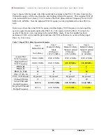


L M K 0 4 9 0 6 E V A L U A T I O N B O A R D O P E R A T I N G I N S T R U C T I O N S
SNAU126
18
Connector Name
Signal Type,
Input/Output
Description
Test point:
CLKin0_SEL_TP
CLKin1_SEL_TP
CMOS,
Input/Output
Programmable status I/O pins. By default, set as input
pins for controlling input clock switching of CLKin0
and CLKin1.
These inputs will not be functional because
CLKin_Select_MODE is set to 0 (CLKin0 Manual) by
default in the
Bits/Pins
tab in CodeLoader. To enable
input clock switching, CLKin_Select_MODE must be
3 or 6 and Status_CLKinX_TYPE must be 0 to 3 (pin
enabled as an input).
Input Clock Switching – Pin Select Mode
When CLKin_SELECT_MODE is 3, the
Status_CLKinX pins select which clock input is active
as follows:
Status_CLKin1 Status_CLKin0
Active Clock
0
0
CLKin0
0
1
CLKin1
1
0
CLKin2
1
1
Holdover
Input Clock Switching – Auto with Pin Select
When CLKin_SELECT_MODE is 6, the active clock is
selected using the Status_CLKinX pins upon an input
clock switch event as follows:
Status_CLKin1 Status_CLKin0
Active
Clock
X
0
CLKin0
1
0
CLKin1
0
0
Reserved
Refer to the
LMK04906 Family Datasheet
section
“Input Clock Switching” for more information.
Status Outputs
When Status_CLKinX_TYPE is 3 to 6 (pin enabled as
an output), the status output signal for the
corresponding Status_CLKinX pin can be programmed
on the
Bits/Pins
tab via the Status_CLKinX_MUX
control.
Refer to the
LMK04906 Family Datasheet
section
“Status Pins” for more information.


