MSP430xG461x
MIXED SIGNAL MICROCONTROLLER
SLAS508I − APRIL 2006 − REVISED MARCH 2011
56
POST OFFICE BOX 655303
•
DALLAS, TEXAS 75265
electrical characteristics over recommended operating free-air temperature (unless otherwise
noted) (continued)
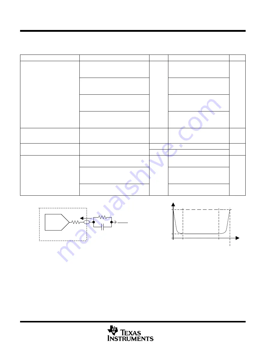
12-bit DAC, output specifications
PARAMETER
TEST CONDITIONS
V
CC
MIN
TYP
MAX
UNIT
No Load, Ve
REF+
= AV
CC
,
DAC12_xDAT = 0h, DAC12IR = 1,
DAC12AMPx = 7
0
0.005
V
Output voltage
range
No Load, Ve
REF+
= AV
CC
,
DAC12_xDAT = 0FFFh, DAC12IR = 1,
DAC12AMPx = 7
2 2 V/3 V
AV
CC
−0.05
AV
CC
V
V
O
range
(see Note 1,
Figure 29)
R
Load
= 3 k
Ω
, Ve
REF+
= AV
CC
,
DAC12_xDAT = 0h, DAC12IR = 1,
DAC12AMPx = 7
2.2 V/3 V
0
0.1
V
R
Load
= 3 k
Ω
, Ve
REF+
= AV
CC
,
DAC12_xDAT = 0FFFh, DAC12IR = 1,
DAC12AMPx = 7
AV
CC
−0.13
AV
CC
C
L(DAC12)
Max DAC12
load
capacitance
2.2V/3V
100
pF
I
Max DAC12
2.2V
−0.5
+0.5
mA
I
L(DAC12)
Max DAC12
load current
3V
−1.0
+1.0
mA
R
Load
= 3 k
Ω
, V
O/P(DAC12)
<
0.3 V,
DAC12AMPx = 2, DAC12_xDAT = 0h
150
250
R
O/P(DAC12)
Output
resistance
(see Figure 29)
R
Load
= 3 k
Ω
,
V
O/P(DAC12)
>
AV
CC
−0.3 V
DAC12_xDAT = 0FFFh
2.2 V/3 V
150
250
Ω
(
g
)
R
Load
= 3 k
Ω
,
0.3V
≤
V
O/P(DAC12)
≤
AV
CC
− 0.3V
1
4
NOTE 1: Data is valid after the offset calibration of the output amplifier.
RO/P(DAC12_x)
Max
0.3
AVCC
AVCC −0.3V
VOUT
Min
RLoad
AVCC
CLoad = 100pF
2
ILoad
DAC12
O/P(DAC12_x)
Figure 29. DAC12_x Output Resistance Tests
Summary of Contents for MSP430CG4616IPZ
Page 110: ......