J721E EVM Hardware Architecture
62
SPRUIS4A – December 2019 – Revised May 2020
Copyright © 2019–2020, Texas Instruments Incorporated
Jacinto7 J721E/DRA829/TDA4VM Evaluation Module (EVM)
To PCIe Card Wi-Fi/BT:
The downstream port1 of USB HUB is connected to the Wi-Fi/BT header (J2) on the CP board. The power
to the WiFi header is provided through current limit load switch with integrated ESD protection device
TPD3S014DBVR. The power is controlled by USB hub power enable signal USB1_DN1_PE.
To Stacked Connector:
The downstreams port2 and 3 of USB HUB is connected to the stacked USB 2.0 Type-A receptacle AU-
Y1008-2 on the CP board. The power to the USB Type-A receptacle is provided through current limit load
switch with integrated ESD protection device TPD3S014DBVR for each port. The power is controlled by
USB hub power enable signals USB1_DN2_PE and USB1_DN3_PE.
To Expansion Connector:
The downstream port4 of USB HUB is connected to EVM Expansion connector. The current version of
EVM is not supporting any peripherals on this port. It is reserved for future development.
4.12.3
USB 3.0 Micro AB Interface (Reserved Port)
This is an optional interface provided for a future version of the J7 SoC only; it is not supported in the
J721E EVM.
4.13 CAN Interface
The four CAN ports of J721E SoC (MCU_MCAN0, MCU_MCAN1, MCAN0, and MCAN2) is supported on
the Common Processor board as explained below.
MCU CAN0
The MCU CAN0 port of J721E SoC is connected to the CAN transceiver with Wake function supported
device TCAN1043-Q1. A 2-pin header J29 (68002-202HLF) is provided inline for user probe option.
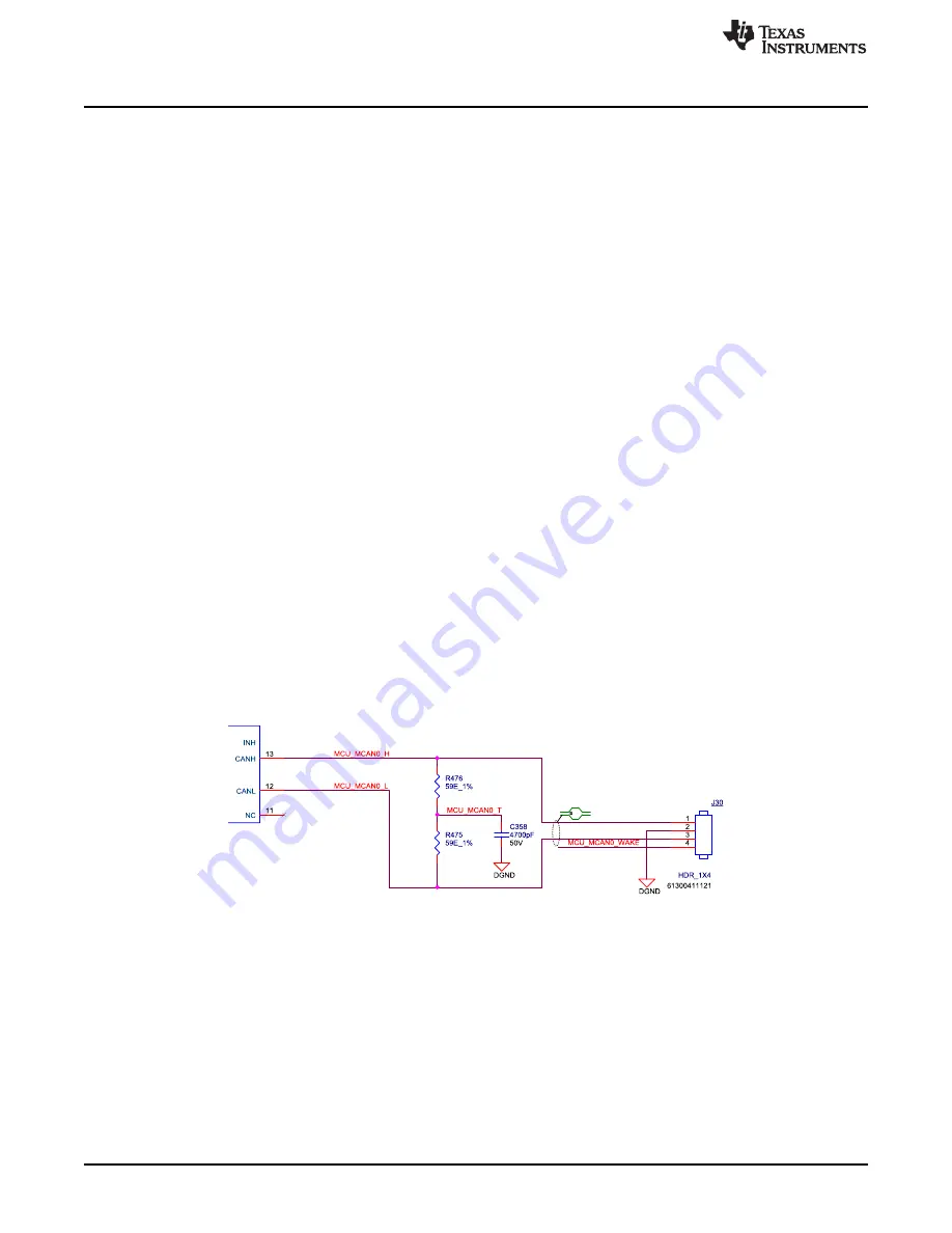
The output of the CAN transceiver is terminated to a 4-pin header J30 (61300411121).
The signals MCU_MCAN0_H and MCU_MCAN0_L are routed as differential signals with 120E impedance
with split termination. This Split termination improves the electromagnetic emissions behavior of the
network by eliminating fluctuations in the bus common-mode voltages at the start and end of message
transmissions.
Figure 46. MCU CAN0 Interface
VSYS_MCU_5V0 to the CAN transceiver is generated using a Step-Up converter TPS61240DRV by
giving VSYS_3V3 as input supply to the converter.
The STB signal is an active low signal held low with integrated pull down by default.
Hardware WAKEn input for the CAN interface is provided using a push-button SW12 available on the
Common processor board bottom left corner. However, the MCU_CAN0 wake feature is disabled by
default (resistor population). Only CAN wake-up supported is from MAIN domain.


