Texas Instruments ISO5852SDWEVM-017 User Manual Download Page 14

Test Setup and Results

www.ti.com

14

SLLU298 – May 2018

Submit Documentation Feedback

Copyright © 2018, Texas Instruments Incorporated

ISO5852SDW Driving and Protecting SiC and IGBT Power Modules

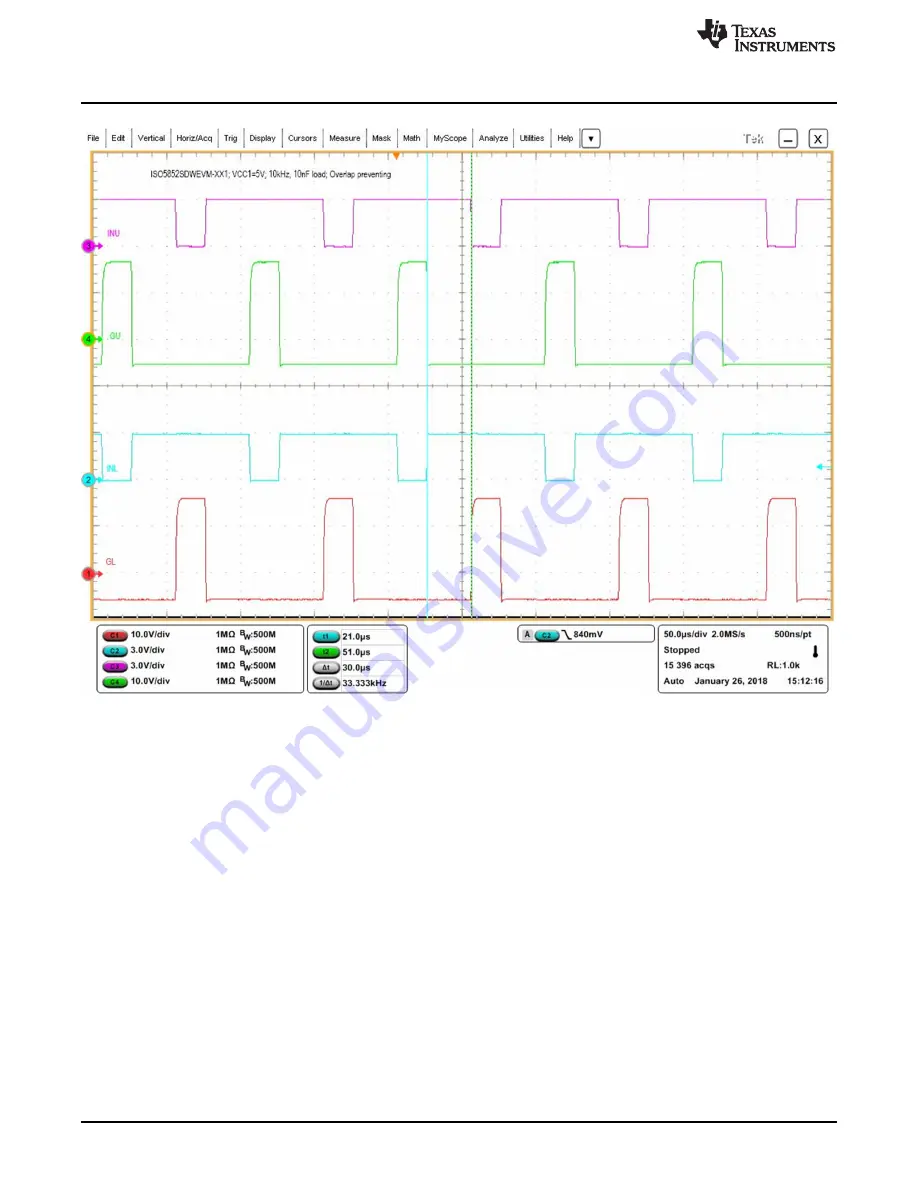
Figure 6. Major Input and Output Waveforms Using Output Overlapping Prevention Feature

INU (pink) is high side input: 3.0V/div

OU (green) is high side output: 10V/div

INL (blue) is low side input: 3.0V/div

OL (red) is low side output: 10V/div

Time scale is 50µs/div

Summary of Contents for ISO5852SDWEVM-017

Page 1: ...hematic 25 4 2 Bill of Materials 31 List of Figures 1 ISO5852SDWEVM 017 EVM Block Diagram 6 2 ISO5852SDWEVM 017 Top View 8 3 ISO5852SDWEVM 017 Mounted on Top of Power Module 9 4 Power Up and Bias Supply Voltages VU and VL Test Setup 11 5 Test Setup for Input and Output Switching Waveforms 12 6 Major Input and Output Waveforms Using Output Overlapping Prevention Feature 14 7 Thermistor Amplifier Te...

Page 2: ...iC and IGBT Power Modules 1 Electrical Specifications 4 2 Voltages and Current During Power Up Test 12 3 Function Generator Settings 13 4 Oscilloscope Settings 13 5 Themistor Amplifier Output Signals 15 6 Input Bus Voltage Sense Amplifier Outputs 16 7 Bill of Materials 31 Trademarks All trademarks are the property of their respective owners ...

Page 3: ...ding connector height allows direct connection to standard 62 mm half bridge modules 1 1 Features This EVM supports the following features 20 A peak split sink and source drive current to optimize turn on and turn off switching time Two 2 W output bias supplies with undervoltage lockout UVLO and overvoltage lockout OVLO protection Turn ON and turn OFF drive voltages can be programmed independently...

Page 4: ...CCOF Vcc falling OVLO threshold 5 4 5 5 V VCCOH Vcc UVLO hysteresis 0 2 V VCC2U VCC2L Turn ON drive voltages Transformer 750342879 15 17 19 V VCC2U VCC2L Turn OFF drive voltages Transformer 750313734 5 9 5 4 7 V DRIVE CURRENT AND POWER IOH Peak source current CLOAD 10nF 15 20 A IOL Peak sink current CLOAD 10nF 15 20 A PDRV Drive power per channel At 25 C 2 0 W INPUT OUTPUT SIGNALS VINR VRSTR INL I...

Page 5: ...wn to 4 V 8 3 9 0 9 5 V TDESATBLN K Blanking time 310 400 480 ns TDS90 Response time to 90 VOUTHL CLOAD 10nF 553 760 ns TDS10 Response time to 10 VOUTHL CLOAD 10nF 2 3 5 µs ICHARGE Capacitor charge current 0 42 0 5 0 58 mA IDISCHARGE Capacitor discharge current 9 14 mA VCLAMP Miller clamp threshold 1 6 2 1 2 5 V ICLAMP Miller clamp current 4 A ISOLATION CMTI CMTI 100 V ns VISO Withstand isolation ...

Page 6: ...2 V 9 V 500 µA STO VCC2 Ready Fault 10 10 Vdrp2 Vdrn1 VCC Logic Block Inv Rec 15 V Vdrp1 S1 Vdrn1 DC DC VCC Rx Tx Reinforced Isolation 10 10 S1 S2 VCC 5 V AMC1301 Vdrn2 VCC 5 V Vdrp1 BUS_P BUS_N VCC_5V GND INU FU RST INL FL F TRO_P TRO_N DU SU GU DL SL GL TR_N DU TR_P 5 V Overview www ti com 6 SLLU298 May 2018 Submit Documentation Feedback Copyright 2018 Texas Instruments Incorporated ISO5852SDW D...

Page 7: ...vice This driver has all necessary short circuit protection features including desaturation current sensing soft short circuit turn OFF Miller gate clamp fault power ready and reset signals 1 3 4 Split Rail Bias Supply using SN6505B Split rail bias supply generates 17V turn ON and 5V turn OFF voltages using two push pull transformer drivers SN6505B operating at 424kHz and housed in 6 pin small SOT...

Page 8: ...onitoring using thermistor inside the module and AMC1301 amplifier 1 3 7 Isolated Differential Amplifier AMC1301 The AMC1301 is a precision isolated amplifier with an output separated from the input circuitry by an isolation barrier providing protection from electromagnetic and electrical noise in the system The input of the AMC1301 device is optimized for sensing signals in 250 mV range with high...

Page 9: ...VM it will typically be in a stand alone configuration separate from power module This EVM does not internally generate high voltages or high temperatures In the start up configuration there will be no high voltage or high temperature capable of presenting the user with an electrical shock hazard or burn resulting from elevated temperature risks provided the EVM is used within its electrical load ...

Page 10: ... pin 17 to BUS_N pin 18 and TRO_P pin 20 to TRO_N pin 19 diagnostic signals must be strictly monitored to assure both high voltage and thermal protective features are being utilized The user is required to provide necessary interface controller hardware to shut down and deenergize the system immediately if BUS_P to BUS_N signal exceeds 1 85 VDC or signal TRO_P to TRO_N drops below 0 135 VDC 2 2 Eq...

Page 11: ...ent measurements with expected range up to 500 mA Here and in all test setups below red arrows indicate positive terminals and black arrows indicate return terminal Figure 4 Power Up and Bias Supply Voltages VU and VL Test Setup WARNING Before start testing make sure to follow all electrical safety and ESD protection requirements implemented at your company 1 Enable power supply PS1 2 Gradually in...

Page 12: ... Icc MM2 VU MM3 VU MM5 VL MM6 VL 2 95 V 3 05 V 30 mA 0 1 V 0 1 V 0 1 V 0 1 V 4 65 V 4 75 V 130 mA 145 mA 15 5 V 16 5 V 4 5 V 5 2 V 15 4 V 16 4 V 4 5 V 5 2 V 4 95 V 5 05 V 135 mA 150 mA 16 8 V 17 5 V 5 0 V 5 5 V 16 6 V 17 4 V 5 0 V 5 5 V 5 4 V 5 45 V 140 mA 155 mA 17 5 V 19 0 V 5 5 V 6 2 V 17 3 V 18 8 V 5 5 V 6 2 V 5 7 V MM4 6 V 30 mA 0 1 V 0 1 V 0 1 V 0 1 V 2 2 2 Input and Output Switching Wavefor...

Page 13: ...CHANNEL VERTICAL SCALE HORIZONTAL SCALE BANDWIDTH COUPLING TERMINATIO N SYNC TRIGGER RESOLUTION Ch 1 red 10 V div 50 µs div 500 MHz or above DC 1 MΩ High Ch 2 blue 3 V div Ch 2 Ch 3 pink 3 V div Ch 4 green 10 V div 1 Enable power supply PS1 2 Gradually increase the voltage at PS1 into 4 95 V to 5 05 V range and monitor current using MM1 that should not exceed 150 mA 3 Enable channel A ch 1 and cha...

Page 14: ...rporated ISO5852SDW Driving and Protecting SiC and IGBT Power Modules Figure 6 Major Input and Output Waveforms Using Output Overlapping Prevention Feature INU pink is high side input 3 0V div OU green is high side output 10V div INL blue is low side input 3 0V div OL red is low side output 10V div Time scale is 50µs div ...

Page 15: ...ly PS1 2 Gradually increase the voltage at PS1 into 4 95 V to 5 05 V range and monitor current using MM1 that should not exceed 150 mA 3 Set resistances using Resistance Decade Box in accordance to Table 5 and monitor voltages at MM5 and MM6 4 Gradually reduce the voltage of power supply PS1 down to 0 V and disable it Table 5 Themistor Amplifier Output Signals RESISTANCE 5 0 kΩ 2 0 kΩ 800 Ω 280 Ω ...

Page 16: ... and monitor current using MM1 that should not exceed 145 mA 3 Enable power supply PS2 4 Gradually increase the voltage of power supply PS2 from 0 V up to 300 V and monitor voltages in accordance to Table 6 5 Gradually decrease the voltage of power supply PS2 down to 0 and disable it 6 Gradually reduce the voltage of power supply PS1 down to 0 V and disable it Table 6 Input Bus Voltage Sense Ampli...

Page 17: ...ts 17 SLLU298 May 2018 Submit Documentation Feedback Copyright 2018 Texas Instruments Incorporated ISO5852SDW Driving and Protecting SiC and IGBT Power Modules Figure 9 Safety Isolated Regions between High and Low Voltage Board Areas ...

Page 18: ...Copyright 2018 Texas Instruments Incorporated ISO5852SDW Driving and Protecting SiC and IGBT Power Modules 3 Board Layout General top and bottom view component placement and all four layers are shown in Figure 10 through Figure 16 respectively Figure 10 Top View of the Board ...

Page 19: ...com Board Layout 19 SLLU298 May 2018 Submit Documentation Feedback Copyright 2018 Texas Instruments Incorporated ISO5852SDW Driving and Protecting SiC and IGBT Power Modules Figure 11 Bottom View Of The Board ...

Page 20: ...d Layout www ti com 20 SLLU298 May 2018 Submit Documentation Feedback Copyright 2018 Texas Instruments Incorporated ISO5852SDW Driving and Protecting SiC and IGBT Power Modules Figure 12 Component Placement ...

Page 21: ...www ti com Board Layout 21 SLLU298 May 2018 Submit Documentation Feedback Copyright 2018 Texas Instruments Incorporated ISO5852SDW Driving and Protecting SiC and IGBT Power Modules Figure 13 Top Layer ...

Page 22: ...ard Layout www ti com 22 SLLU298 May 2018 Submit Documentation Feedback Copyright 2018 Texas Instruments Incorporated ISO5852SDW Driving and Protecting SiC and IGBT Power Modules Figure 14 Signal Layer 1 ...

Page 23: ...w ti com Board Layout 23 SLLU298 May 2018 Submit Documentation Feedback Copyright 2018 Texas Instruments Incorporated ISO5852SDW Driving and Protecting SiC and IGBT Power Modules Figure 15 Signal Layer 2 ...

Page 24: ...oard Layout www ti com 24 SLLU298 May 2018 Submit Documentation Feedback Copyright 2018 Texas Instruments Incorporated ISO5852SDW Driving and Protecting SiC and IGBT Power Modules Figure 16 Bottom Layer ...

Page 25: ...s depending on applications By default the board set into output overlapping protection mode Removing resistor shunts R48 and R52 allows output overlapping When attaching EVM to power module it is recommended to remove output load capacitors C16 and C36 To set turn ON and OFF output driver voltages beoynd the default UVLO OVLO protection can be disabled by removing resistor R53 By removing resisti...

Page 26: ...erials www ti com 26 SLLU298 May 2018 Submit Documentation Feedback Copyright 2018 Texas Instruments Incorporated ISO5852SDW Driving and Protecting SiC and IGBT Power Modules Figure 17 Electrical Schematic of ISO5852SDWEVM 017 ...

Page 27: ...of Materials 27 SLLU298 May 2018 Submit Documentation Feedback Copyright 2018 Texas Instruments Incorporated ISO5852SDW Driving and Protecting SiC and IGBT Power Modules Figure 18 Electrical Schematic with Functional Blocks Outlined ...

Page 28: ...ules Additional waveforms are shown below to illustrate described above adjustments and EVM drive current capabilites Operation waveforms with overlapping enabled is shown in Figure 19 Figure 19 Waveforms with Overlapping Enabled INU pink is high side input 3 0V div OU green is high side output 10V div INL blue is low side input 3 0V div OL red is low side output 10V div Time scale is 50µs div ...

Page 29: ...Current capability during turn ON is illustrated in Figure 20 by rise time while charging 10 nF load capacitors Figure 20 Rise Time and Propagation Delay Waveforms with 10 nF Load INU pink is high side input 3 0V div OU green is high side output 10V div INL blue is low side input 3 0V div OL red is low side output 10V div Time scale is 50ns div Rise time is about 30 ns Propagation delay is 133 5 n...

Page 30: ...wer Modules Current capability during turn OFF with 10 nF load capacitors is illustrated in Figure 21 Figure 21 Fall Time and Propagation Delay Waveforms with 10 nF Load INU pink is high side input 3 0V div OU green is high side output 10V div INL blue is low side input 3 0V div OL red is low side output 10V div Time scale is 50ns div Fall time is about 34 ns Propagation delay is 98 5 ns ...

Page 31: ...0603 C41 C49 2 0 1uF 12061C104JAT2A AVX CAP CERM 0 1 uF 100 V 5 X7R 1206 1206 C42 1 0 01uF C0402C103J5RACTU Kemet CAP CERM 0 01 uF 50 V 5 X7R 0402 0402 C46 C47 C57 C58 4 10pF 04025U100CAT2A AVX CAP CERM 10 pF 50 V 2 5 C0G NP0 AEC Q200 Grade 1 0402 0402 C50 1 0 01uF C0603H103J3GACTU Kemet CAP CERM 0 01 uF 25 V 5 C0G NP0 0603 0603 C54 C56 2 2 2uF C1206C225K4RACTU Kemet CAP CERM 2 2 uF 16 V 10 X7R 12...

Page 32: ...k CRCW0402523KFKED Vishay Dale RES 523 k 1 0 063 W AEC Q200 Grade 0 0402 0402 R49 R50 R51 R54 R58 R59 R62 R66 8 10 0 CRCW040210R0FKED Vishay Dale RES 10 0 1 0 063 W 0402 0402 R53 1 10 5k CRCW040210K5FKED Vishay Dale RES 10 5 k 1 0 063 W AEC Q200 Grade 0 0402 0402 R55 R60 2 0 CRCW04020000Z0ED Vishay Dale RES 0 5 0 063 W AEC Q200 Grade 0 0402 0402 R56 1 40 2k CRCW040240K2FKED Vishay Dale RES 40 2 k ...

Page 33: ...y set forth above or credit User s account for such EVM TI s liability under this warranty shall be limited to EVMs that are returned during the warranty period to the address designated by TI and that are determined by TI not to conform to such warranty If TI elects to repair or replace such EVM TI shall have a reasonable time to repair such EVM or provide replacements Repaired EVMs shall be warr...

Page 34: ...the user guide with the maximum permissible gain and required antenna impedance for each antenna type indicated Antenna types not included in this list having a gain greater than the maximum gain indicated for that type are strictly prohibited for use with this device Concernant les EVMs avec antennes détachables Conformément à la réglementation d Industrie Canada le présent émetteur radio peut fo...

Page 35: ...ed loads Any loads applied outside of the specified output range may also result in unintended and or inaccurate operation and or possible permanent damage to the EVM and or interface electronics Please consult the EVM user guide prior to connecting any load to the EVM output If there is uncertainty as to the load specification please contact a TI field representative During normal operation even ...

Page 36: ...COST OF REMOVAL OR REINSTALLATION ANCILLARY COSTS TO THE PROCUREMENT OF SUBSTITUTE GOODS OR SERVICES RETESTING OUTSIDE COMPUTER TIME LABOR COSTS LOSS OF GOODWILL LOSS OF PROFITS LOSS OF SAVINGS LOSS OF USE LOSS OF DATA OR BUSINESS INTERRUPTION NO CLAIM SUIT OR ACTION SHALL BE BROUGHT AGAINST TI MORE THAN TWELVE 12 MONTHS AFTER THE EVENT THAT GAVE RISE TO THE CAUSE OF ACTION HAS OCCURRED 8 2 Specif...

Page 37: ... TI Resource NO OTHER LICENSE EXPRESS OR IMPLIED BY ESTOPPEL OR OTHERWISE TO ANY OTHER TI INTELLECTUAL PROPERTY RIGHT AND NO LICENSE TO ANY TECHNOLOGY OR INTELLECTUAL PROPERTY RIGHT OF TI OR ANY THIRD PARTY IS GRANTED HEREIN including but not limited to any patent right copyright mask work right or other intellectual property right relating to any combination machine or process in which TI product...

Reviews: