background image

1

Features

2

General Description

3

Signal Path and Control

User's Guide

SCAU024 – September 2008

Low Phase Noise Clock Evaluation Module — up to 1.5

GHz

Easy-to-use evaluation module to generate low
phase noise clocks up to 1.5 GHz

Easy device programming via host-powered USB
port

Rapid configuration through provided EVM Control
Software

Can be powered from the USB port, or by an
external 3.3V power supply

Single-ended or differential input; external crystal
can be used with on-chip oscillator

Footprint for optional crystal filter on one output

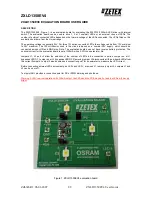
Figure 1. CDCE62005EVM Evaluation Board

The CDCE62005 is a high performance, low phase noise frequency synthesizer and jitter cleaner. It
features an on-chip PLL with dual integrated LC Voltage Controlled Oscillators (VCOs) operating from
1.75–2.35 GHz. It provides support for three manually or automatically selected inputs, and provides up to
five differential, or ten single-ended, low-jitter outputs.

The CDCE62005 supports single-ended and differential input signals, as well as providing a crystal
oscillator circuit that operates in conjunction with an external AT-cut crystal.

The CDCE62005 is programmed through an SPI interface using the supplied EVM programming graphical
user interface (GUI).

The evaluation module (EVM) demonstrates the electrical performance of the device. This
fully-assembled, factory-tested evaluation board allows complete validation of all device functions. For
optimum performance, the board is equipped with 50

SMA connectors and well-controlled 50

impedance microstrip transmission lines.

The CDCE62005 provides three selectable inputs – PRI REF, SEC REF, and AUX IN. The PRI REF and
SEC REF inputs can accept up to 1500 MHz in the fan-out mode. In the PLL mode, PRI REF and SEC
REF can accept an input at up to 500MHz from a differential signal source, or up to 250MHz from a single

SCAU024 – September 2008

Low Phase Noise Clock Evaluation Module — up to 1.5 GHz

1

Submit Documentation Feedback

Summary of Contents for CDCE62005EVM

Page 1: ...des up to five differential or ten single ended low jitter outputs The CDCE62005 supports single ended and differential input signals as well as providing a crystal oscillator circuit that operates in...

Page 2: ...the LVPECL output The corresponding load resistor must be selected in the software interface when an output is configured as LVPECL The LVCMOS outputs can operate at frequencies up to 250MHz The LVPEC...

Page 3: ...ocation browse to the CDCE62005EVM program file folder that was used during instillation If Windows does not ask for a driver no action is needed After USB driver installation the EVM software should...

Page 4: ...vider Input type Input selection PFD Charge Pump Internal External Loop Filter Output MUX selection Output Divider and Output type Other configurations are selected by the software with user selectabl...

Page 5: ...art MUX The Smart MUX section of the EVMCS can be clicked for a popup window that opens as shown in Figure 4 showing Selections on the EECLKSEL option 0 suggests using the REF_SEL pin for input select...

Page 6: ...be selected from the allowable dropdown list for each component Figure 6 Loop Filter Internal Only Alternately the loop filter with additional external components can be enabled by clicking the Use Ex...

Page 7: ...e outputs can be clicked to open a popup window that shows options for each output clock source These are selectable between LVPECL High Swing LVPECL in which cases the output 150 termination is autom...

Page 8: ...his configuration the USB microcontroller is powered by the USB port 5V supply while the CDCE62005 is powered by the 3 3V external supply This configuration is best for programming the CDCE62005 while...

Page 9: ...lable options on the CDCE62005EVM using the dip switches SW9 and SW10 located at the bottom side of the EVM and shown below Figure 11 External Loop Filter Selection Switches Configuration for PLL Lock...

Page 10: ...uF 1 2 C29 33pF C29 33pF 1 2 R138 4 7k R138 4 7k 1 2 R129 4 7k R129 4 7k 1 2 R110 10k R110 10k D8 MBRS2040LT3 D8 MBRS2040LT3 1 2 R7 33 R7 33 1 2 R144 10k R144 10k 1 2 R5 15k R5 15k 3 1 2 Q1 2N2222A Q1...

Page 11: ...5 SW10 TDA04H0SK1 SW10 TDA04H0SK1 1 2 R88 5 1 R88 5 1 C106 10uF C106 10uF 1 2 R76 5 1 R76 5 1 C116 100uF C116 100uF C105 1uF C105 1uF 1 2 R75 NP 1 09K R75 NP 1 09K C109 4 7uF X5R NP C109 4 7uF X5R NP...

Page 12: ...F C120 0 1uF 1 2 R223 150 R223 150 1 2 R229 0 NP R229 0 NP C119 0 1uF C119 0 1uF 1 2 R213 150 R213 150 Q56 FDV303N Q56 FDV303N 1 2 R222 10k R222 10k C131 0 1uF C131 0 1uF Q57 FDV303N Q57 FDV303N C130...

Page 13: ...4 RESET 14 VCC1_PLL 5 VCC2_PLL 42 SEC_REF 3 SEC_REF 2 VCC_IN 1 PRI_REF 45 PRI_REF 46 VCC_IN 47 VBB 48 EXT_LFP 40 AUX_IN 43 EXT_LFN 41 PLL_LOCK 37 VCC_VCO 35 THERMAL_PAD 49 U5 CDCE62005 U5 CDCE62005 C1...

Page 14: ...F C80 0 1uF C80 0 1uF OE 1 VCC 6 NC OUTN 5 OUT OUTP 4 GND 3 NC 2 U12 PE7745DU 30 72M U12 PE7745DU 30 72M C77 0 1uF C77 0 1uF C58 1uF C58 1uF 1 2 R130 49 9 R130 49 9 C78 0 1uF C78 0 1uF 1 3 2 JP_3_6 JP...

Page 15: ...TIES EXPRESSED IMPLIED OR STATUTORY INCLUDING ANY WARRANTY OF MERCHANTABILITY OR FITNESS FOR ANY PARTICULAR PURPOSE The user assumes all responsibility and liability for proper and safe handling of th...

Page 16: ...ting any load to the EVM output If there is uncertainty as to the load specification please contact a TI field representative During normal operation some circuit components may have case temperatures...

Page 17: ...siness practice TI is not responsible or liable for any such statements TI products are not authorized for use in safety critical applications such as life support where a failure of the TI product wo...

Reviews: