background image

Chapter 2: Installation

2-3

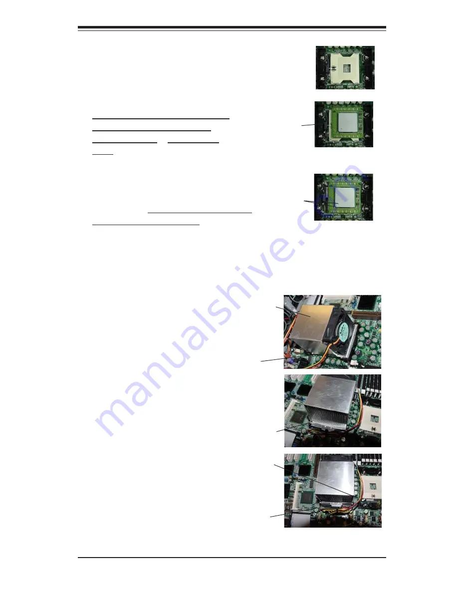
5. Lift the lever on the CPU socket:

lift the lever completely or you will

damage the CPU socket when

power is applied

  (Install CPU1

first.)

6. Install the CPU in the socket marked

"CPU1".  Make sure that pin 1 of the CPU is

seated on pin 1 of the socket (both corners

are marked).  When using only one CPU,

install it into CPU socket #1 (CPU socket #2 is

automatically disabled if only one CPU is

used).

7. Press the lever down until

you hear it *click* into the

locked position.

4. Secure the other retention

bracket into position by

repeating Step 3.

8. Apply the proper amount of thermal

compound to the CPU die and place

the heatsink and fan on top of the

CPU.

Heatsink

 9. Secure the heatsink by locking the

retention clips into their proper

position.

 10. Connect the three wires of

the CPU fan to the respective CPU

fan connector.

CPU fan

connector

CPU fan

w i r e s

Retention clip

CPU

Socket lever

Pin 1

 11. Repeat this procedure to

install a second CPU in CPU

socket #2.

Summary of Contents for X5DA8

Page 1: ... SUPER X5DA8 SUPER X5DAE SUPER X5DAL G SUPER X5DAL TG2 USER S MANUAL Revision 1 1c SUPER ...

Page 2: ...BILITY TO USE THIS PRODUCT OR DOCUMENTATION EVEN IF ADVISED OF THE POSSIBILITY OF SUCH DAMAGES IN PARTICULAR THE VENDOR SHALL NOT HAVE LIABILITY FOR ANY HARDWARE SOFTWARE OR DATA STORED OR USED WITH THE PRODUCT INCLUDING THE COSTS OF REPAIRING REPLACING INTEGRATING INSTALLING OR RECOVERING SUCH HARDWARE SOFTWARE OR DATA Any disputes arising between manufacturer and customer shall be governed by th...

Page 3: ... begins with instructions on handling static sensitive devices Read this chapter when you want to install the processor and DIMM memory modules and when mounting the motherboard in the chassis Also refer to this chapter to connect the floppy and hard disk drives the IDE interfaces the parallel and serial ports the keyboard and mouse the power supply and various control panel buttons and indicators...

Page 4: ... Super X5DAL TG2 Layout 1 14 Super X5DAL TG2 Quick Reference 1 15 Motherboard Features 1 16 Intel E7505 Chipset System Block Diagram 1 18 1 2 Chipset Overview 1 19 1 3 Special Features 1 19 BIOS Recovery 1 19 Recovery from AC Power Loss 1 19 1 4 PC Health Monitoring 1 20 1 5 ACPI Features 1 21 1 6 Power Supply 1 23 1 7 Super I O 1 23 Chapter 2 Installation 2 1 Static Sensitive Devices 2 1 Precauti...

Page 5: ...oard and Mouse Ports 2 11 Fan Headers 2 12 Power LED Speaker Header JD1 2 12 Third Power Supply Fail Header 2 12 Wake On LAN 2 13 Wake On Ring 2 13 JSLED 2 13 Keylock 2 13 2 6 Jumper Settings 2 14 Explanation of Jumpers 2 14 CMOS Clear 2 14 SCSI Enable Disable 2 14 GLAN Enable Disable 2 15 Power Fail Alarm Enable Disable 2 15 CPU Chassis CPU Fan Select 2 15 System Bus Speed 2 15 USB Wake Up 2 16 W...

Page 6: ...ng 3 1 Troubleshooting Procedures 3 1 Before Power On 3 1 No Power 3 1 No Video 3 1 Memory Errors 3 2 Losing the System s Setup Configuration 3 2 3 2 Technical Support Procedures 3 2 3 3 Frequently Asked Questions 3 3 3 4 Returning Merchandise for Service 3 5 Chapter 4 BIOS 4 1 Introduction 4 1 4 2 Running Setup 4 2 4 3 Main BIOS Setup 4 2 4 4 Advanced Setup 4 6 4 5 Security Setup 4 16 4 6 Boot Se...

Page 7: ...listed here is damaged or missing contact your retailer One 1 Supermicro Mainboard One 1 ribbon cable for IDE devices One 1 floppy ribbon cable One 1 four port USB 2 0 cable retail only Two 2 Pentium 4 Xeon active heatsinks FAN 050 T retail single package for X5DA8 X5DAE only Two 2 heatsink retention clips SKT 095 604E Two 2 Xeon mounting plates SKT 120 P X5DAL G TG2 only One 1 I O backpanel shiel...

Page 8: ...o com Europe Address SuperMicro Computer B V Het Sterrenbeeld 28 5215 ML s Hertogenbosch The Netherlands Tel 31 0 73 6400390 Fax 31 0 73 6416525 Email sales supermicro nl General Information support supermicro nl Technical Support rma supermicro nl Customer Support Asia Pacific Address SuperMicro Taiwan D5 4F No 16 Chien Ba Road Chung Ho 235 Taipei Hsien Taiwan R O C Tel 886 2 8226 3990 Fax 886 2 ...

Page 9: ...Chapter 1 Introduction 1 3 Introduction Notes ...

Page 10: ...1 4 Introduction SUPER X5DA8 X5DAE X5DAL G X5DAL TG2 User s Manual Figure 1 1 SUPER X5DA8 Image ...

Page 11: ...Chapter 1 Introduction 1 5 Introduction Figure 1 2 SUPER X5DAE Image ...

Page 12: ...1 6 Introduction SUPER X5DA8 X5DAE X5DAL G X5DAL TG2 User s Manual Figure 1 3 SUPER X5DAL G Image ...

Page 13: ...Chapter 1 Introduction 1 7 Introduction Figure 1 4 SUPER X5DAL TG2 Image ...

Page 14: ...3 MHz PCI 4 133 MHz PCI X 3 100 MHz PCI X 2 100 MHz PCI X 1 IDE 2 IDE 1 FLOPPY Ultra III LVD SCSI CH A BIOS MCH AIC 7902 ICH4 Speaker 8xAGP 1 5V COM1 COM2 ATX PWR CONN J15 DIMM 1B DIMM 1A DIMM 2B DIMM 2A DIMM 3B DIMM 3A BANK 1 BANK 2 BANK 3 JF2 JP36 CPU1 Chassis Fan JP9 JP8 JP7 J2 J3 CPU2 Chassis Fan Chassis Fan1 JA1 JA2 Ultra III LVD SCSI CH B Chassis Fan2 JD4 J12 JP40 FPUSB 2 3 WOL JWOR1 JP35 JD...

Page 15: ...mary ATX Power Connector CD1 CD2 Audio CD Input large small COM1 COM2 COM1 COM2 Serial Port Connector CPU CHS OH FAN CPU Chassis Overheat Fan Headers DIMM 1A DIMM 3B Memory RAM Slots FPUSB0 1 2 3 Front Panel USB Headers GLAN G bit Ethernet Port J2 J3 IDE1 2 Hard Disk Drive Connector J7 Parallel Printer Port J9 PS 2 Keyboard Mouse Ports J12 IR CIR Header J15 Processor Power Connector J30 Power Conn...

Page 16: ... 1 Overheat Fan CPU Fan1 CD1 CD2 CPU Fan2 33 MHz PCI 5 33 MHz PCI 4 133 MHz PCI X 3 100 MHz PCI X 2 100 MHz PCI X 1 IDE 2 IDE 1 FLOPPY BIOS MCH AIC 7902 ICH4 Speaker 8xAGP 1 5V COM1 COM2 ATX PWR CONN J15 DIMM 1B DIMM 1A DIMM 2B DIMM 2A DIMM 3B DIMM 3A BANK 1 BANK 2 BANK 3 JF2 JP36 CPU1 Chassis Fan JP9 JP8 JP7 J2 J3 CPU2 Chassis Fan Chassis Fan1 Chassis Fan2 JD4 J12 JP40 FPUSB 2 3 WOL JWOR1 JP35 JD...

Page 17: ...ctor CD1 CD2 Audio CD Input large small COM1 COM2 COM1 COM2 Serial Port Connector CPU CHS OH FAN CPU Chassis Overheat Fan Headers DIMM 1A DIMM 3B Memory RAM Slots FPUSB0 1 2 3 Front Panel USB Headers GLAN G bit Ethernet Port J2 J3 IDE1 2 Hard Disk Drive Connector J7 Parallel Printer Port J9 PS 2 Keyboard Mouse Ports J12 IR CIR Header J15 Processor Power Connector J30 Power Conn for use with AGP Pr...

Page 18: ...2 CPU 1 Overheat Fan CPU Fan1 CPU Fan2 33 MHz PCI 2 33 MHz PCI 1 100 MHz PCI X 2 133 MHz PCI X 1 IDE 2 IDE 1 FLOPPY BIOS MCH ICH4 8xAGP 1 5V COM1 COM2 ATX PWR CONN J15 DIMM 1 DIMM 2 DIMM 3 DIMM 4 BANK 0 BANK 1 Chassis Fan 1 JP9 JP8 JP7 J2 J3 FPUSB 2 3 WOL JP35 JD1 FPUSB 0 1 JL1 S UPER X5DAL G I O BRIDGE JP39 JBT1 JPUSB JPWAKE JP36 JOH1 JP37 JF2 Chassis Fan 2 JPL1 JP38 JWOR1 J12 D3 D4 Jumpers not n...

Page 19: ... Power Connector COM1 COM2 COM1 COM2 Serial Port Connector CPU CHS OH FAN CPU Chassis Overheat Fan Headers DIMM 1 DIMM 4 Memory RAM Slots FPUSB0 1 2 3 Front Panel USB Headers GLAN G bit Ethernet Port J2 J3 IDE1 2 Hard Disk Drive Connector J7 Parallel Printer Port J9 PS 2 Keyboard Mouse Ports J12 IR CIR Header J15 Processor Power Connector J30 Power Conn for use with AGP Pro cards JD1 PWR LED Speak...

Page 20: ...an2 33 MHz PCI 2 33 MHz PCI 1 100 MHz PCI X 2 66 MHz PCI 1 IDE 2 IDE 1 FLOPPY BIOS MCH ICH4 8xAGP 1 5V COM1 COM2 ATX PWR CONN J15 DIMM 1 DIMM 2 DIMM 3 DIMM 4 BANK 0 BANK 1 Chassis Fan 1 JP9 JP8 JP7 J2 J3 FPUSB 2 3 WOL JD1 FPUSB 0 1 S UPER X5DAL TG2 I O BRIDGE JP39 JBT1 JPUSB JPWAKE JP36 JOH1 JP37 JF2 Chassis Fan 2 JPL1 JP38 JWOR1 J12 D3 D4 JPA1 JPA2 SATA 1 SATA 2 SATA 3 SATA 4 SATA Cntrlr JSLED JL...

Page 21: ... ATX Power Connector COM1 COM2 COM1 COM2 Serial Port Connector CPU CHS OH FAN CPU Chassis Overheat Fan Headers DIMM 1 DIMM 4 Memory RAM Slots FPUSB0 1 2 3 Front Panel USB Headers GLAN G bit Ethernet Port J2 J3 IDE1 2 Hard Disk Drive Connector J7 Parallel Printer Port J9 PS 2 Keyboard Mouse Ports J12 IR CIR Header J15 Processor Power Connector J30 Power Conn for use with AGP Pro cards JD1 PWR LED S...

Page 22: ... requires memory modules to be installed in pairs See Section 2 3 for details Chipset Intel E7505 chipset Expansion Slots X5DA8 X5DAE X5DAL G X5DAL TG2 One 64 bit 133 MHz PCI X One 64 bit 133 MHz PCI X Two 64 bit 100 MHz PCI X One 64 bit 100 MHz PCI X Two 32 bit 33 MHz PCI Two 32 bit 33 MHz PCI One 8xAGP Pro 1 5V One 8xAGP Pro 1 5V This is a 64 bit 66 MHz PCI slot on the X5DAL TG2 BIOS 4 Mb Phoeni...

Page 23: ...DAL TG2 Zero channel Serial ATA RAID support green slot X5DAL TG2 Intel 82545EM Gb Ethernet controller Intel EW82546EB dual Gb Ethernet controller X5DAL TG2 2 EIDE Ultra DMA 100 bus master interfaces 1 floppy port interface up to 2 88 MB 2 Fast UART 16550A compatible serial ports 1 EPP ECP Parallel Port PS 2 mouse and PS 2 keyboard ports Up to 6 USB 2 0 Universal Serial Bus ports AC 97 Audio CODEC...

Page 24: ...xAGP PCI X 1 PCI X 2 SCSI PCI X 3 GLAN 100 MHz PCI X Bus 100 MHz PCI X Bus P64H2 PCI X 1 Serial ATA PCI X 2 GLAN 133 66 DAL G DAL TG2 MHz PCI X PCI Bus 100 MHz PCI X Bus X5DA8 X5DAE X5DAL G X5DAL TG2 SATAfor X5DAL TG2 only PCI 1 on X5DAL TG2 Figure 1 9 Intel E7505 Chipset System Block Diagram Note This is a general block diagram Please see the previous Motherboard Features pages for details on the...

Page 25: ... O Controller Hub provides various integrated functions including a two channel Ultra ATA 100 bus master IDE controller USB 2 0 host con trollers an integrated LAN controller a System Management Bus controller and an AC 97 compliant interface The P64H2 PCI X Hub provides a 16 bit connection to the MCH for high performance IO capability and two independent 64 bit PCI X interfaces 1 3 Special Featur...

Page 26: ...ans are controlled by the power manage ment functions The thermal fan is controlled by the overheat detection logic Environmental Temperature Control The thermal control sensor monitors the CPU temperature in real time and will turn on the thermal control fan whenever the CPU temperature exceeds a user defined threshold The overheat circuitry runs independently from the CPU It can continue to moni...

Page 27: ...V to 3 5V This will allow the regulator to run cooler and thus make the system more stable 1 5 ACPI Features ACPI stands for Advanced Configuration and Power Interface The ACPI specification defines a flexible and abstract hardware interface that pro vides a standard way to integrate power management features throughout a PC system including its hardware operating system and application soft ware ...

Page 28: ...ill spin down Depressing the power button again will cause the whole system to wake up During the SoftOff state the ATX power supply provides power to keep the re quired circuitry in the system alive In case the system malfunctions and you want to turn off the power just depress and hold the power button for 4 seconds This option can be set in the Power section of the BIOS Setup routine External M...

Page 29: ...y a few minutes of operation See Section 2 5 for details on connecting the power supply cables It is strongly recommended that you use a high quality power supply that meets ATX power supply Specification 2 02 or above It must also be SSI compliant info at http www ssiforum org Additionally in areas where noisy power transmission is present you may choose to install a line filter to shield the com...

Page 30: ...Mb s which support higher speed modems The Super I O supports one PC compatible printer port SPP Bi directional Printer Port BPP Enhanced Parallel Port EPP or Extended Capabilities Port ECP The Super I O provides functions that comply with ACPI Advanced Con figuration and Power Interface which includes support of legacy and ACPI power management through an SMI or SCI function pin It also features ...

Page 31: ...removing the board from the anti static bag Handle the board by its edges only do not touch its components periph eral chips memory modules or gold contacts When handling chips or modules avoid touching their pins Put the motherboard and peripherals back into their antistatic bags when not in use For grounding purposes make sure your computer chassis provides ex cellent conductivity between the po...

Page 32: ...nel of a chassis that has four mounting holes as shown on right White pegs 4 2 Insert the white pegs into the black anchors Do not force the white pegs all the way in only about 1 3 of the way into the black anchors 3 Place a retention bracket in the proper position and secure it by pressing pegs into two of the retention holes until you hear a click The clicking sound indicates that the peg is lo...

Page 33: ...abled if only one CPU is used 7 Press the lever down until you hear it click into the locked position 4 Secure the other retention bracket into position by repeating Step 3 8 Apply the proper amount of thermal compound to the CPU die and place the heatsink and fan on top of the CPU Heatsink 9 Secure the heatsink by locking the retention clips into their proper position 10 Connect the three wires o...

Page 34: ...he chassis match Although a chassis may have both plastic and metal mounting fasteners metal ones are highly recommended because they ground the motherboard to the chassis Make sure the metal standoffs click in or are screwed in tightly Then use a screwdriver to secure the motherboard onto the motherboard tray Lever Processor installed Triangle Triangle Empty socket Warning Make sure you lift the ...

Page 35: ...r of DIMMs into the memory slots starting with Bank 1 The memory scheme is interleaved so you must install two modules at a time beginning with Bank 1 then Bank 2 and so on 2 Insert each DIMM module vertically into its slot Pay attention to the notch along the bottom of the module to prevent inserting the DIMM module incorrectly 3 Gently press down on the DIMM module until it snaps into place in t...

Page 36: ...s are color coded in conformance with the PC 99 specification See Figure 2 3 below for the colors and locations of the various I O ports Figure 2 3 I O Port Locations and Definitions Mouse Green Keyboard Purple USB Ports COM1 Port Turquoise GLAN COM2 Port Turquoise Line In Blue MIC Pink Line Out Lime Note The Line In Line Out and MIC ports are not included on the X5DAL G and X5DAL TG2 The X5DAL TG...

Page 37: ... designed specifically for use with Supermicro server chassis See Figure 2 4 for the descriptions of the various control panel buttons and LED indicators Refer to the following section for descriptions and pin defini tions Figure 2 4 JF2 Header Pins Power Button Overheat LED 1 NIC1 LED Reset Button 2 Power Fail LED HDD LED Power LED Reset Pwr Vcc Vcc Vcc Vcc Ground Ground 19 20 Vcc X Ground NMI X ...

Page 38: ...rset ATX 24 pin specifica tion however it also supports a 20 pin power supply connector Make sure that the orientation of the connector is correct See the table on the right for pin defini tions Pins 1 thru 4 5 thru 8 Definition Ground 12v 8 Pin 12v Power Supply Connector J15 NMI Button The non maskable interrupt button header is located on pins 19 and 20 of JF2 Refer to the table on the right for...

Page 39: ...1 and 12 of JF2 Attach the NIC LED cable to display network activity Refer to the table on the right for pin definitions HDD LED The HDD LED connection is located on pins 13 and 14 of JF2 Attach the hard drive LED cable here to display disk activity for any hard drives on the system including SCSI Serial ATA and IDE See the table on the right for pin defini tions HDD LED Pin Definitions JF2 Pin Nu...

Page 40: ...al Serial Bus USB0 1 Two USB 2 0 ports are located beside the PS 2 keyboard mouse ports USB0 is the bottom connec tor and USB1 is the top connector See the table on the right for pin definitions Universal Serial Bus Pin Definitions Pin Number Definition 1 5V 2 P0 3 P0 4 Ground 5 N A Pin Number Definition 1 5V 2 P0 3 P0 4 Ground 5 Key USB0 USB1 Reset Button The Reset Button connection is lo cated o...

Page 41: ... table at right for pin definitions See Figure 2 3 for the locations of each PS 2 Keyboard and Mouse Port Pin Definitions J9 Pin Number 1 2 3 4 5 6 Definition Data NC Ground VCC Clock NC Serial Ports The COM1 and COM2 serial ports are located under the parallel port see Figure 2 3 See the table on the right for pin definitions Serial Port Pin Definitions COM1 COM2 Pin Number Definition 1 CD 2 RD 3...

Page 42: ...ED Speaker On the JDI header pins 1 3 are for a power LED and pins 4 7 are for the speaker See the table on the right for speaker pin defini tions Note The speaker connec tor pins are for use with an exter nal speaker If you wish to use the onboard speaker you should close pins 6 7 with a jumper Speaker Connector Pin Definitions JD1 Pin Number 4 5 6 7 Function Key Definition Red wire Speaker data ...

Page 43: ... in suspend state See the table on the right for pin definitions You must have a Wake On Ring card and cable to use this feature Wake on Ring Pin Definitions JWOR Pin Number 1 2 Definition Ground W ake up Keylock The keyboard lock connection is lo cated on JP35 Utilizing this header allows you to inhibit any actions made on the keyboard effectively locking it JSLED X5DAL TG2 only The JSLED header ...

Page 44: ...The SCSI Termination jumper at JP34 allows you to enable or dis able the onboard SCSI controller The normal default position is on pins 1 2 to enable terminate the onboard SCSI See the table on the right for jumper settings Jumper Position Pins 1 2 Pins 2 3 Definition Enabled Disabled SCSI Enable Disable Jumper Settings JP34 CMOS Clear JBT1 is used to clear CMOS Instead of pins this jumper consist...

Page 45: ...ve one or two power supply units in stalled you should disable this with JP9 to prevent false alarms See the table on the right for jumper settings The default set ting is disabled Jumper Position Open Closed Definition Disabled Enabled Power Fail Alarm Enable Disable Jumper Settings JP9 CPU Chassis CPU Fan Select not on X5DAL G X5DAL TG2 JP33 allows you to select to use ei ther the CPU fan or the...

Page 46: ...m up with a USB keyboard that has been connected to a USB port not header Set JPUSB to pins 1 2 to support USB keyboard wake up and resume from ACPI S1 mode and pins 2 3 pins to support USB keyboard wake up and resume from ACPI S3 mode See the table on the right for jumper settings Note Your power supply must provide 5v of standby voltage with at least 1A to use this feature Watch Dog JP37 control...

Page 47: ...n trols channel B The default setting is open to enable teminate both SCSI channels See the table on the right for jumper settings Note In order for the SCSI drives to function properly please do not change the default setting set by the manufacturer Jumper Position Open Closed Definition Enabled Disabled SCSI Channel Termination Enable Disable Jumper Settings JPA1 JPA2 Serial ATA Enable Disable X...

Page 48: ...higher and supply 720mA of standby power to use this fea ture Jumper Position 1 2 2 3 Definition Disabled Enabled Keyboard Wake Up Jumper Settings JPWAKE System Bus Speed JP39 allows you to select Auto 400 or 533 MHz for your system front side bus speed The recommended Auto setting will automatically deter mine the system bus speed of your processor s See the table on the right for jumper settings...

Page 49: ...ted right behind the parallel port behind the mouse keyboard ports on the X5DAL G X5DAL TG2 and are based on Intel pre defined temperature thresholds Hot is a warning that the tem perature is getting too high Therm when lit indicates that power for the corresponding CPU has been shut down See the table at right for the functions as sociated with each LED Onboard Overheat LEDs D1 D4 LED D1 D2 D3 D4...

Page 50: ...ppy disk drives The connector with twisted wires always connects to drive A and the connector that does not have twisted wires always connects to drive B Parallel Printer Port Connector The parallel printer port is lo cated on J7 See the table on the right for pin definitions Pin Number Function 1 Strobe 3 Data Bit 0 5 Data Bit 1 7 Data Bit 2 9 Data Bit 3 11 Data Bit 4 13 Data Bit 5 15 Data Bit 6 ...

Page 51: ...30 Read Data 32 Side 1 Select 34 Diskette Floppy Connector Pin Definitions JP7 Pin Number Function 1 Reset IDE 3 Host Data 7 5 Host Data 6 7 Host Data 5 9 Host Data 4 11 Host Data 3 13 Host Data 2 15 Host Data 1 17 Host Data 0 19 GND 21 DRQ3 23 I O W rite 25 I O Read 27 IOCHRDY 29 DACK3 31 IRQ14 33 Addr 1 35 Addr 0 37 Chip Select 0 39 Activity Pin Number Function 2 GND 4 Host Data 8 6 Host Data 9 ...

Page 52: ...23 24 25 26 27 28 29 30 31 32 33 34 Signal Names DB 12 DB 13 DB 14 DB 15 DB P1 DB 0 DB 1 DB 2 DB 3 DB 4 DB 5 DB 6 DB 7 DB P GROUND GROUND TERMPW R TERMPW R RESERVED GROUND ATN GROUND BSY ACK RST MSG SEL C D REQ I O DB 8 DB 9 DB 10 DB 11 Connector Contact Number 35 36 37 38 39 40 41 42 43 44 45 46 47 48 49 50 51 52 53 54 55 56 57 58 59 60 61 62 63 64 65 66 67 68 68 pin Ultra320 160 SCSI Connectors ...

Page 53: ...ting this CD into your CDROM drive the display shown in Figure 2 4 should appear If this dis play does not appear click on the My Computer icon and then on the icon representing your CDROM drive Finally double click on the S Setup icon Click the icons showing a hand writing on paper to view the readme files for each item The bottom icon with a CD on it allows you to view the entire contents of the...

Page 54: ...2 24 SUPER X5DA8 X5DAE X5DAL G X5DAL TG2 User s Manual Notes ...

Page 55: ...he keyboard and mouse 3 Remove all add on cards 4 Install one CPU making sure it is fully seated and connect the chassis speaker and the power LED to the motherboard Check all jumper settings as well No Power 1 Make sure no short circuits exist between the motherboard and the chas sis 2 Verify that all jumpers are set to their default positions 3 Check that the 115V 230V switch on the power supply...

Page 56: ...y should know of any possible problem s with the specific system configuration that was sold to you NOTE If you are a system integrator VAR or OEM a POST diagnos tics card is recommended For I O port 80h codes refer to App B Memory Errors 1 Make sure the DIMM modules are properly and fully installed 2 Determine if different speeds of DIMMs have been installed and verify that the BIOS setup is conf...

Page 57: ...port department We can be reached by e mail at support supermicro com or by fax at 408 503 8000 option 2 3 3 Frequently Asked Questions Question What are the various types of memory that my mother board can support Answer The X5DA8 X5DAE supports up to 12 GB of registered ECC DDR 266 200 PC2100 1600 memory The X5DAL G X5DAL TG2 supports up to 8 GB of registered ECC or unbuffered DDR 266 200 PC2100...

Page 58: ... the system from a Windows boot disk Type A phlash B X5DA8 Bin s x mode 3 mfg BIOS filename rom or A phx7505 BIOS filename rom The system will flash BIOS from here and reboot once it finishes To recover BIOS a recovery flash requires an update key over the COM port as follows hardwire Pin4 wires to Pin8 and Pin9 Pin7 wires to Pin6 Pin3 wires to Pin2 and leave Pin 1 and Pin 5 open Use the Supermicr...

Page 59: ...the manufacturer the RMA number should be prominently displayed on the outside of the shipping carton and mailed prepaid or hand carried Shipping and handling charges will be ap plied for all orders that must be mailed when service is complete This warranty only covers normal consumer use and does not cover dam ages incurred in shipping or from failure due to the alternation misuse abuse or improp...

Page 60: ...3 6 SUPER X5DA8 X5DAE X5DAL G X5DAL TG2 User s Manual Notes ...

Page 61: ...ry requires very little electrical power When the computer is turned off a back up battery provides power to the BIOS flash chip enabling it to retain system parameters Each time the computer is powered on the computer is configured with the values stored in the BIOS ROM by the system BIOS which gains control at boot up How To Change the Configuration Data The CMOS information that determines the ...

Page 62: ...ays 1 By pressing Delete immediately after turning the system on or 2 When the message shown below appears briefly at the bottom of the screen during the POST Power On Self Test press the Delete key to activate the main Setup menu Press the Delete key to enter Setup 4 3 Main BIOS Setup All main Setup options are described in this section The main BIOS Setup screen is displayed below Use the Up Dow...

Page 63: ...enter the correct data Press the Enter key to save the data Phoenix BIOS Setup Utility Main Advanced Security Boot Exit System Time 16 36 44 System Date 10 20 02 Legacy Diskette A 1 44 1 25 MB Legacy Diskette B Disabled Primary Master 120 GB Primary Slave None Secondary Master CD ROM Secondary Slave None System Memory 256 MB Extended Memory 3967 KB Item Specific Help F1 Help Select Item Change Val...

Page 64: ...rimary Master Primary Slave Secondary Master Secondary Slave These settings allow the user to set the parameters of the IDE Primary Master Slave and IDE Secondary Master Slave slots Hit Enter to activate the following sub menu screen for detailed options of these items Set the correct configurations accordingly The items included in the sub menu are Phoenix BIOS Setup Utility Main Advanced Securit...

Page 65: ...ill access the IDE Primary Master Device via LBA mode The options are Enabled and Disabled 32 bit I O Selects 32 bit I O operation Options are Enabled and Disabled Transfer Mode Selects the transfer mode Options are Standard Fast PIO1 Fast PIO2 Fast PIO3 Fast PIO4 FPIO3 DMA1 and FPIO4 DMA2 Ultra DMA Mode Selects Ultra DMA Mode Options are Disabled Mode 0 Mode 1 Mode 2 Mode 3 Mode 4 and Mode 5 Syst...

Page 66: ...nu to make changes to the following settings Quick Boot Mode If enabled this feature will speed up the POST Power On Self Test routine after the computer is turned on The settings are Enabled and Disabled If Disabled the POST routine will run at normal speed Quiet Boot This setting allows you to Enable or Disable the diagnostic screen during boot up Phoenix BIOS Setup Utility Main Advanced Securit...

Page 67: ...an unexpected loss of power Options are Stay On Power Off and Last State Watch Dog This setting is for enabling the Watch Dog feature The options are Enabled and Disabled Multiprocessor Specification This setting allows you to configure the multiprocessor specification revision level The options are 1 1 and 1 4 NT4 Installation Workaround This setting allows BIOS to provide a workaround for the ab...

Page 68: ...is setting to change the speed of the onboard SCSI and PCI X slots 1 and 2 Options are Auto 33 MHz 66 MHz 100 MHz and 133 MHz Frequency for PCIX 3 GLAN Use this setting to change the speed of the onboard LAN and PCI X slot 3 Options are Auto 33 MHz 66 MHz 100 MHz and 133 MHz PCI Device Slot 1 Slot 5 Access the submenu for each of the five settings above to make changes to the following Option ROM ...

Page 69: ...ws you to turn off system RAM to free up address space The options for this setting are Disabled and Extended ECC Configuration This setting lets you enable or disable ECC Error Correction and Checking The options are ECC and Disabled ECC Error Type This setting lets you select which type of interrupt will be activated as a result of an ECC error The options are None NMI Non Maskable Interrupt SMI...

Page 70: ...bled Local Bus IDE Adapter Use this setting to enable the integrated local bus IDE adapter Options are Disable Primary Secondary and Both USB Device 9 Function 7 This setting controls USB functionality Options are Disabled and Enabled SMART Monitoring Self Monitoring Analysis and Reporting Technology SMART can help predict impending drive failures Select Auto to allow BIOS to auto detect hard disk...

Page 71: ...R for an infrared device Base I O Address Select the base I O address for serial port B The options are 3F8 2F8 3E8 and 2E8 Interrupt Select the IRQ interrupt request for serial port B Options are IRQ3 and IRQ4 Parallel Port This setting allows you to assign control of the parallel port The options are Enabled user defined Disabled and Auto BIOS controlled Base I O Address Select the base I O addr...

Page 72: ...t the base I O address for the parallel port The options are Primary and Secondary Advanced Processor Options Access the submenu to make changes to the following settings CPU Speed This is a display that indicates the speed of the installed processor Frequency Ratio This setting allows you to specify the value of the internal frequency multiplier of the processor which is used to determine the pro...

Page 73: ...y not a setting informing you of the event log validity Event Log Capacity This is a display not a setting informing you of the event log capacity View DMI Event Log Highlight this item and press Enter to view the contents of the event log Event Logging This setting allows you to Enable or Disable event logging ECC Event Logging This setting allows you to Enable or Disable ECC event logging Mark D...

Page 74: ...K 38 4K 57 6K and 115 2K Console Type Choose from the available options to select the console type for console redirection Flow Control Choose from the available options to select the flow control for console redirection Console Connection Select the console connection either Direct or Via Modem Continue CR after POST Choose whether to continue with console redirection after the POST routine Optio...

Page 75: ...Chapter 4 BIOS 4 15 System Temperature CPU Fan1 CPU Fan2 Chassis Fan 1 Chassis Fan 2 Processor Vcore 3 3V Standby 3 3V Vcc 5V Vcc 12V Vcc 1 8V Vcc 12V Vcc ...

Page 76: ... means such a password has not been used and Set means a supervisor password has been entered for the system User Password Is This displays whether a user password has been entered for the system Clear means such a password has not been used and Set means a user password has been entered for the system Phoenix BIOS Setup Utility Main Advanced Security Boot Exit Supervisor Password Is Clear User Pa...

Page 77: ... When prompted type the user s password in the dialogue box to set or to change the user s password which allows access to the system at boot up Password on Boot This setting allows you to require a password to be entered when the system boots up Options are Enabled password required and Disabled password not required Fixed Disk Boot Sector This setting may offer some protection against viruses wh...

Page 78: ...d press Enter to expand the field See details on how to change the order and specs of devices in the Item Specific Help window CD ROM Drive See details on how to change the order and specs of the CD ROM drive in the Item Specific Help window Hard Drive Highlight and press Enter to expand the field See details on how to change the order and specs of hard drives in the Item Specific Help window Phoe...

Page 79: ...Changes Item Specific Help F1 Help Select Item Change Values F9 Setup Defaults Esc Exit Select Menu Enter Select Sub Menu F10 Save and Exit Exit Saving Changes Highlight this item and hit Enter to save any changes you made and to exit the BIOS Setup utility Exit Discarding Changes Highlight this item and hit Enter to exit the BIOS Setup utility without saving any changes you may have made Load Set...

Page 80: ...s Manual Discard Changes Highlight this item and hit Enter to discard cancel any changes you made You will remain in the Setup utility Save Changes Highlight this item and hit Enter to save any changes you made You will remain in the Setup utility ...

Page 81: ...led Keyboard controller failed test May require replacing keyboard controller Keyboard locked Unlock key switch Unlock the system to proceed Monitor type does not match CMOS Run SETUP Monitor type not correctly identified in Setup Shadow Ram Failed at offset nnnn Shadow RAM failed at offset nnnn of the 64k block at which the error was detected System RAM Failed at offset nnnn System RAM failed at ...

Page 82: ...sed Previous POST did not complete successfully POST loads default values and offers to run Setup If the failure was caused by incorrect values and they are not corrected the next boot will likely fail On systems with control of wait states improper Setup settings can also terminate POST and cause this error on the next boot Run Setup and verify that the waitstate configuration is correct This err...

Page 83: ...ftware NMI Failed ServerBIOS2 test error Cannot generate software NMI Non Maskable Interrupt Fail Safe Timer NMI Failed ServerBIOS2 test error Fail Safe Timer takes too long device Address Conflict Address conflict for specified device Allocation Error for device Run ISA or EISA Configuration Utility to resolve resource conflict for the specified device CD ROM Drive CD ROM Drive identified Enterin...

Page 84: ...es successfully tested nnnn kB System RAM Passed Where nnnn is the amount of system RAM in kilobytes successfully tested One or more I2O Block Storage Devices were excluded from the Setup Boot Menu There was not enough room in the IPL table to display all installed I2O block storage devices Operating system not found Operating system cannot be located on either drive A or drive C Enter Setup and s...

Page 85: ... Write down and follow the information shown on the screen Press F2 to enter Setup Optional message displayed during POST Can be turned off in Setup PS 2 Mouse PS 2 mouse identified Run the I2O Configuration Utility One or more unclaimed block storage devices have the Configuration Request bit set in the LCT Run an I2O Configuration Utility e g the SAC utility System BIOS shadowed System BIOS copi...

Page 86: ...A 6 SUPER X5DA8 X5DAE X5DAL G X5DAL TG2 User s Manual Notes ...

Page 87: ...write the error in the top left corner of the screen The following is a list of codes that may be written to port 80h Appendix B BIOS POST Codes POSTCode Description 02h Verify Real Mode 03h Disable Non Maskable Interrupt NMI 04h Get CPU type 06h Initialize system hardware 07h Disable shadow and execute code from the ROM 08h Initialize chipset with initial POST values 09h Set IN POST flag 0Ah Init...

Page 88: ...down 38h Shadow system BIOS ROM 3Ah Auto size cache 3Ch Advanced configuration of chipset registers 3Dh Load alternate registers with CMOS values 41h Initialize extended memory for RomPilot 42h Initialize interrupt vectors 45h POST device initialization 46h 2 1 2 3 Check ROM copyright notice 47h Initialize I20 support 48h Check video configuration against CMOS 49h Initialize PCI bus and devices 4A...

Page 89: ... 80h Disable onboard Super I O ports and IRQs 81h Late POST device initialization 82h Detect and install external RS232 ports 83h Configure non MCD IDE controllers 84h Detect and install external parallel ports 85h Initialize PC compatible PnP ISA devices 86h Re initialize onboard I O ports 87h Configure Motherboard Configurable Devices optional 88h Initialize BIOS Data Area 89h Enable Non Maskabl...

Page 90: ... Terminate QuietBoot optional B6h Check password optional B7h Initialize ACPI BIOS B9h Prepare Boot BAh Initialize SMBIOS BBh Initialize PnP Option ROMs BCh Clear parity checkers BDh Display MultiBoot menu BEh Clear screen optional BFh Check virus and backup reminders C0h Try to boot with INT 19 C1h Initialize POST Error Manager PEM C2h Initialize error logging C3h Initialize error display functio...

Page 91: ...mory size EEh Shadow Boot Block EFh System memory test F0h Initialize interrupt vectors F1h Initialize Run Time Clock F2h Initialize video F3h Initialize System Management Manager F4h Output one beep F5h Clear Huge Segment F6h Boot to Mini DOS F7h Boot to Full DOS IftheBIOSdetectserror2C 2E or30 base512KRAMerror itdisplaysanadditional word bitmap xxxx indicating the address line or bits that faile...

Page 92: ...B 6 SUPER X5DA8 X5DAE X5DAL G X5DAL TG2 User s Manual Notes ...

Reviews: