background image

4-4

UP-960(UC)

UP-960CE(CE)

4-1. VIDEO CIRCUIT

4-1-1. Input Trap Filter Circuit

The composite video signal is inputted to MA-91 board from BNC connector (CN1-VIDEO  IN).  75 ohm termination is

turned ON/OFF by dip switch (S501 pin 1).  After that, it is divided three signal systems via input buffer, the signal passed

through trap filter (FL1) for NTSC, the signal passed through trap filter (FL2) for PAL, no processed signal is inputted to

the analog switch (IC1 pins 1, 3 and 5).  Selection of signal is performed by system control (IC505) and inputted to the

video amplifier 1 (IC2 pins 15 and 16).

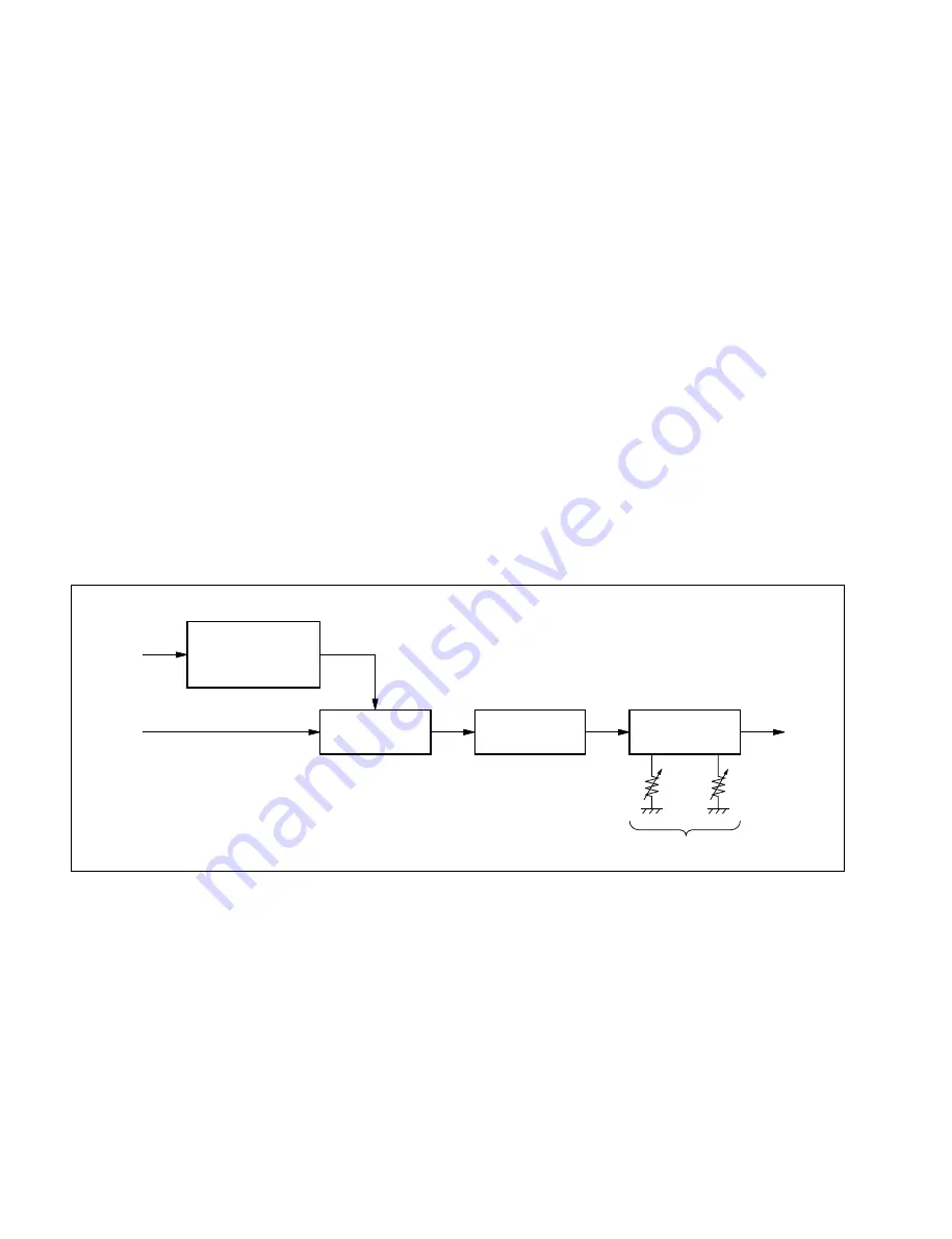
4-1-2. Sharpness, AGC Circuit and C-SYNC Signal

The signal from analog switch (IC1) is divided two systems, one is inputted to the  video amplifier 1 (IC2 pins 15 and 16),

another is inputted to the peak detection circuit for AGC.  Sharpness is switched Soft and Hard by changing the voltage that

is inputted to the video amplifier 1 (IC2 pin 13).  The voltage is switched by analog switch (IC5) and controlled by system

control (IC505).  AGC is performed by using contrast amplifier in the video amplifier 1 (IC2).  When setting AGC to ON,

the voltage is peak voltage of input video signal that is obtained  by peak detection circuit (Q13, Q14, IC4), when setting

AGC to OFF, the reference   voltage is outputted from analog switch (IC5) by controlling system control (IC505), both

voltages are fed back to video amplifier 1 (IC2 pin 11) and controls gain of amplifier. C-SYNC signal is outputted from

video amplifier 1 (IC2 pin 3).  Peak detection circuit for AGC is also used this C-SYNC signal.

Peak Detection Circuit

4-1-3. Brightness, Contrast Control and A/D Conversion

The video signal outputted from video amplifier 1 (IC2 pin 10) is inputted to video amplifier 2 (IC6 pin 16) via low pass

filter (Q6, Q7).  The voltages obtained by each volume on the front panel are inputted to video amplifier 2 (IC6 pins 4 and

6).  And BRIGHTNESS and CONTRAST adjustments are performed according to this voltages. After that, adjusted signal

outputted from video amplifier 2 (IC6 pin 9) is converted to digital signal at A/D converter (IC7) and it is stored to the

memory.

C-SYNC

VIDEO

Q11, Q12

Q13

Q14

IC2

RV2

RV3

GAIN ADJUSTMENT

IC5-

!=

CLAMP

PULSE

GENERATOR

PEDESTAL

CLAMP

INTEGRATION

CIRCUIT

VIDEO

AMP

Summary of Contents for UP-960

Page 1: ...VIDEO GRAPHIC PRINTER UP 960 UP 960CE 1st Edition SERVICE MANUAL ...

Page 2: ...d service personnel only To reduce the risk of electric shock fire or injury do not perform any servicing other than that contained in the operating instructions unless you are qualified to do so Refer all servicing to qualified service personnel ...

Page 3: ... CIRCUIT OPERATION DESCRIPTION 4 1 VIDEO CIRCUIT 4 4 4 1 1 Input Trap Filter Circuit 4 4 4 1 2 Sharpness AGC Circuit and C SYNC Signal 4 4 4 1 3 Brightness Contrast Control and A D Conversion 4 4 4 2 OSCILLATOR CIRCUIT 4 5 4 3 IC601 PERIPHERAL CIRCUIT 4 5 4 3 1 Serial Data Reading from System Control 4 6 4 3 2 Writing to the Frame Memory 4 6 4 3 3 Transfer from Frame Memory to Line Memory 4 6 4 3 ...

Page 4: ...N UP DOWN IS OUT OF ORDER 5 4 5 5 PAPER FEEDING IS OUT OF ORDER 5 5 5 6 DOOR OPENING CLOSING IS OUT OF ORDER 5 6 6 SEMICONDUCTOR PIN ASSIGNMENTS SEMICONDUCTOR INDEX 6 1 DIODE 6 2 LED 6 2 TRANSISTOR 6 2 OTHERS 6 2 IC 6 3 7 SPARE PARTS 7 1 NOTES ON REPAIR PARTS 7 1 7 2 EXPLODED VIEW 7 2 Ornamental Block Mechanical Block 7 2 Ornamental Block Switching Regulator 7 3 Sub Assy Top Chassis 7 4 Feeder Blo...

Page 5: ...3 UP 960 UC UP 960CE CE 9 PRINTED WIRING BOARDS AND SCHEMATIC DIAGRAMS MA 91 9 1 KY 421 9 11 PTC 98 9 11 SE 441 9 11 SE 442 9 11 SE 485 9 11 SU 41 9 11 SU 42 9 11 FRAME 9 12 ...

Page 6: ......

Page 7: ...960 UC UP 960CE CE SECTION 1 OPERATING INSTRUCTIONS This section is extracted from operation manual UP 960 UP 960CE 1998 by Sony Corporation Instructions for Use Page 30 EN 3 862 477 01 1 Video Graphic Printer ...

Page 8: ...Symbol on the products This symbol indicates the equipotential terminal which brings the various parts of a system to the same potential For the customers in the U S A This equipment has been tested and found to comply with the limits for a Class A digital device pursuant to Part 15 of the FCC Rules These limits are designed to provide reasonable protection against harmful interference when the eq...

Page 9: ...ted out by using the SCAN DIP switch Fast printing You can make a single printout in about 10 seconds You can make a maximum of 11 copies of the same image continuously Automatic video signal discrimination The type of input video signal EIA or CCIR is automatically discriminated and printed adequately there is no need to change any switch manually Easy and quick paper loading You can load paper j...

Page 10: ... keep this switch set to this position NEGA OFF Makes negative printouts Setting the DIP Switches Preparation O F F 1 2 3 4 5 6 7 8 ON OFF NO FUNCTION ON OFF 1 2 3 4 5 6 7 8 RESERVED RESERVED ON OFF GAMMA POST FEED TONE HARD IMAGE SHARPNESS AGC POSI SOFT NEGA ON OFF TONE TONE 35 3 SHARPNESS switch SOFT ON Normally keep this switch set to this position HARD OFF Obtains greater sharpness of printout...

Page 11: ...lects whether the top or the bottom of the screen is to be printed first NORM ON Normally keep this switch set to this setting Printing is done from the bottom of the screen REV OFF Printing is started from the top of the screen 6 MEMORY switch FRAME ON Normally keep this switch set to this position FIELD OFF When printing fast moving pictures such as a ball being thrown the printout may blur If t...

Page 12: ...lly keep this switch set to this position REV OFF Prints the right and left sides reversed mirror image 0 RESERVED switch Keep this switch set to ON Preparation Setting the DIP Switches Continued 30 3 2 2 3 3 4 3 4 1 3 5 5 3 1 1 3 5 7 7 5 3 1 5 3 1 30 3 2 2 3 3 4 3 4 30 3 2 2 3 3 4 3 4 3 2 3 3 4 4 3 2 5 3 1 30 275 8 7 6 5 4 3 2 1 475 50 250 9 4 5 5 7 5 4 3 3 2 3 2 30 10 7 0 3 30 3 2 2 3 3 4 3 4 1 ...

Page 13: ...33 Is the paper roll loaded properly page 39 Are the DIP switches set correctly page 34 Is the print source being input Making Printouts 1 Press the power ON OFF switch to turn on the printer All buttons on the front panel will light Note Make sure that the PAPER EMPTY indicator is not lit If lit load the paper See page 39 2 Selecting the printing direction and size See Selecting the Printing Dire...

Page 14: ...y the last printout in different sizes Before pressing the COPY button select the printing size as described in Selecting the printing size See page 43 Notes If you press the COPY button immediately after turning the power on the alarm buzzer will sound as nothing is stored in memory In the SMALL mode page 43 if you press the COPY button after you have pressed the PRINT button only once the alarm ...

Page 15: ...eaker Turn the CONTR control counterclockwise To adjust the brightness You can adjust the brightness of printouts using the BRIGHT control To make the brightness brighter Turn the BRIGHT control clockwise To make the brightness darker Turn the BRIGHT control counterclockwise Note You cannot adjust the image once it has been captured in memory Restore an image after adjustment Remotely Controlling ...

Page 16: ...heat sources Avoid locations near radiators or air ducts Also do not subject to direct sunlight or excessive dust humidity mechanical shock or vibration Provide adequate air circulation to prevent heat buildup Do not place the printer on surfaces such as rugs blankets etc or near materials such as curtains and draperies If the printer is subjected to wide and sudden changes in temperature such as ...

Page 17: ...nsert the cleaning sheet into the paper insertion slot Cleaning sheet supplied 2 to 3 cm 49 Paper Type of paper Use only paper specified for this printer The use of other paper may result in reduced printer performance and poor print quality The following types of paper are available UPP 210SE Normal UPP 210HD High density Storing paper Store unused or printed paper in a cool dark place below 30 C...

Page 18: ...s The alarm buzzer sounds White lines or small letters on the screen are not printed clearly Small squares appear over the whole screen The printout is too dark or too light The printout seems stretched Cause remedy When printing with a newly inserted roll of paper dust on the surface of the paper may cause white specks on the printouts n Feed the paper by pressing the FEED button until clean pape...

Page 19: ... 48 Opens or closes the door panel Also interrupts printing midway When the door panel is open the following sub panel appears For details see page 34 DIP switches Others OFF ON ON NO FUNCTION ON OFF 1 2 3 4 5 6 7 8 RESERVED RESERVED ON OFF GAMMA POST FEED TONE HARD IMAGE SHARPNESS AGC POSI SOFT NEGA ON OFF TONE TONE 53 Back 1 VIDEO IN input connector BNC type 33 Connect to the video output connec...

Page 20: ......

Page 21: ...2 1 UP 960 UC UP 960CE CE SECTION 2 SERVICE OVERVIEW 2 1 PC BOARD LOCATION SE 485 Board PTC 98 Board SU 41 Board SU 42 Board SE 443 Board SE 441 Board SE 442 Board MA 91 Board ...

Page 22: ...r and the panels in the numerical order as shown 2 2 1 Removal of the Top Cover 1 Case screws M3 1 Case screws M3 2 Top Cover 2 2 2 Removal of the Door Panel 1 screw BVTT3x6 1 screw BVTT3x6 2 4 3 screw BTP3x8 3 screw BTP3x8 Door Cover Left Door Cover Right 5 CN302 PTC 98 Board Door Panel ...

Page 23: ...aws Front Panel Paper Tray MA 91 Board Press Arms 2 screws PS3x5 3 screws screw M3 with tooth W 3 screws screw M3 with tooth W 1 screw B3x8 Rear Panel NOTE Open the paper tray before removing the front panel For opening the paper tray pull the tray close with the press arm pressed Note on Front Panel Installation Be sure to insert the four claws 6 6 6 6 6 in position 2 2 4 Removal of the Rear Pane...

Page 24: ...s screw M3 with tooth W 1 CN201 1 CN202 1 CN204 1 CN205 1 CN206 1 CN207 1 CN209 1 CN210 MA 91 Board 2 3 REMOVAL OF THE MAIN PARTS NOTE Remove the main parts in the numerical order as shown 2 3 1 Removal of the Mechanical Block Note on Mechanical Block Installation Insert the mechanical assy guide shaft on the chassis into the hole a of the mechanical block 2 3 2 Removal of the MA 91 Board and the ...

Page 25: ...oper 5 Shield Cover 7 Switching Regulator 2 screw BVTT3x6 2 screws BVTT3x6 3 Flat Cables Thermal Head 4 Head Release Arm Top Chassis Assy 1 CN204 SE 441 Board 2 3 3 Removal of the Thermal Head How to rotate the head release arm Pull and rotate the arm in the counterclockwise direction to the position of stopper ...

Page 26: ......

Page 27: ...t Adjustments Specifications 3 1 TRAP ADJUSTMENT Input signal NTSC signal color bar 1410 signal generator PAL signal color bar 1411 signal generator Set rear panel DIP switch pin 2 to ON Adjust FL1 using NTSC color bar input Next adjust FL2 using PAL color bar input TP5 AMP IN MA 91 E 1 Output waveform 1 FL1 MA 91 J 2 1 FL2 MA 91 J 2 The remain of chroma level is the minimum TP5 FL1 FL2 MA 91 ...

Page 28: ...t Adjustments Specifications 3 3 BRIGHTNESS AND CONTRAST ADJUSTMENT Input signal 10 step signal NTSC 1410 signal generator PAL 1411 signal generator In case monitor is not connected set DIP switch pin 1 on the rear panel to ON if connected set to OFF Adjust RV5 C ADJ and RV6 B ADJ using 10 step signal input Set CONT and BRT knobs to the center position on the front panel TP6 AD IN MA 91 E 1 Output...

Page 29: ...oor while it is pushed by hand At that time locked condition measure the voltage and adjust RV401 CN208 pin 9 MA 91 G 3 Output voltage 1 RV401 MA 91 E 4 V1 The voltage when the paper tray is locked by hand during opening or closing of it Approximately 7 5 V V2 V1 2 0V CN208 RV401 MA 91 1 GND V1 V2 Adjust so that the voltage of CN208 pin 8 becomes V2 ...

Page 30: ...or panel DIP switches to ON Set all rear panel DIP switches to ON Set slide switches to NORMAL and STD on the front panel Machine condition for adjustment Adjustments Specifications 3 5 HEAD VOLTAGE ADJUSTMENT 1 VR151 switching regulator Adjust VR151 so that 17 step signal becomes smoothly gradation Switching Regulator right side view front side VR151 1 ...

Page 31: ...rted MEMORY HEAD CONTROL G A Print data is fetched frame memory DRAM Image data on the memory is converted into PWM and sent it to the thermal head FRAME MEMORY DRAM Print data is memorized SYSTEM CONTROL CPU Various blocks are watched and controlled MOTOR DRIVE Motors of head platen cutter fan and door are driven according to the command from system control SENSOR CIRCUIT Sensor values of head pa...

Page 32: ... UP 960 UC UP 960CE CE OVERALL PM HM FM DM HS PS DS MOTOR DRIVE SYSTEM CONTROL CPU MEMORY CONTROL G A AMP FRONT PANEL INPUT CONNECTOR DRAM HEAD VIDEO CIRCUIT SENSOR CIRCUIT BUZZER BOARD CHECKER MA 91 BOARD ...

Page 33: ...BUFFER Q17 BUFFER Q16 MEMORY IC603 REGULATOR REFERENCE Q21 VIDEO AMP 2 IC6 TP1 SYNC 1 2 4 3 7 5 TRAP ON OFF CLKA 31 38 49 68 IC505 SHARPNESS IC505 AGC ON OFF IC505 PEAK DETECTOR IC5 1 2 IC2 Q6 7 IC5 2 2 12 14 13 15 10 16 3 11 13 SYNC 3 5 9 11 4 VIDEO AMP 1 LOW PASS FILTER C SYNC TP5 AMP IN TP6 AD IN TP7 VRT TP8 VRB 16 9 4 6 A D CONVERTER IC7 21 4 11 DA0 DA7 23 14 16 3 19 LOGIC IC IC601 DIOA0 DIOA1...

Page 34: ...erformed by using contrast amplifier in the video amplifier 1 IC2 When setting AGC to ON the voltage is peak voltage of input video signal that is obtained by peak detection circuit Q13 Q14 IC4 when setting AGC to OFF the reference voltage is outputted from analog switch IC5 by controlling system control IC505 both voltages are fed back to video amplifier 1 IC2 pin 11 and controls gain of amplifie...

Page 35: ...12 X601 23 MHz 23 1 21 22 23 25 SCLK SAMPLING CLOCK DELAY IC CXD 8932Q CXD 8726R H SYNC SCLK usual SCLK when fetching Phase matching Phase matching 4 3 IC601 PERIPHERAL CIRCUIT IC601 consists of following blocks 1 Register for serial data storing from system control IC505 1 Various mode setting 22 byte 2 SYNC signal processing parameter 4 byte 3 Coefficient for scaling calculation 128 byte 4 Gamma...

Page 36: ...on of one address is 16 bit FETCH EXTV ODD EVEN WE IMAGE FETCHING PERIOD Frame Unit 4 3 3 Transfer from Frame Memory to Line Memory If COPY pulse is inputted from system control to IC601 pin 128 IC601 performs COPYING signal to L and the print operation is started In order to print selected one line data from frame memory is transferred to one line memory in IC601 IC601 reads necessary print data ...

Page 37: ...SEL 1 REGEN MTPULSE INTV SCK SI 3 4 5 6 207 132 133 134 141 140 139 137 136 10 113 122 10 8 15 8 8x10 8x10 8 8 8 8 4 8 A D CONVERTER INTERPOLATE CALCULATION VIDEO CIRCUIT COEFFICIENT MEMORY FRAME MEMORY FRAME MEMORY CONTROL LINE MEMORY LINE MEMORY CONTROL TEST MODE FILTER THERMAL HEAD STAIR STEP COUNTER THERMAL HEAD CONTROL GAMMA DATA REGISTER PWM COMP x10 NEGA POSI FILTER EXT SYNC SIGNAL PROCESS ...

Page 38: ...ey condition L Pushed H Not pushed 4 4 2 Watch of Various Function Switches IC505 watches settings of various function switches and reflects its settings to the operations Front slide SW Function Operation IC505 pin 88 SMALL L SMALL H NORMAL IC505 pin 89 SIDE L SIDE H STANDARD Front DIP SW Function Operation IC505 pin 23 AGC L ON H OFF IC505 pin 24 IMAGE L POSI H NEGA IC505 pin 25 SHAPNESS L SOFT ...

Page 39: ...e rotation and rotation speed of platen motor by operating driving transistors Q405 406 407 and 408 4 4 4 Head Up and Down Control Up and down motor of the head is driven by IC402 Correct rotation and reverse rotation are possible And their controls are performed by IC505 pins 97 and 98 The head position is detected by optical type head position sensors SE 441 board PH201 and 202 and read by IC505...

Page 40: ... IC505 99pin Operation NEUTRAL L L Neutral CLOSE L H Door is shut OPEN H L Door is opened STOP H H Stopped Condition of Door Position Sensor Door position sensor IC505 85pin IC505 84pin Condition CLOSE L L Door is shut OPEN H L Door is opened In case the door is shut to judge whether door is completely shut or not door position sensor detects and door lock sensor circuit MA 91 board IC404 peripher...

Page 41: ...or The resistor value change of thermistor included in the thermal head is converted to the voltage by IC404 The result is fetched to IC505 pin 78 and is converted A D Cause of this A D converted digital value the density Gamma adjustment fan motor control for head cooling and head in cooling judge by IC601 Gate array are performed 4 4 8 Head Fan Motor for Head Cooling Control Head fan motor is op...

Page 42: ...distinction 4 4 10 Gate Array IC601 Control IC505 transfers operation mode data to gate array IC601 Start and end indication of CAPTURE video signal fetch to the memory operation and COPY memorized image is sent to the head operation are performed CAPTURE Mode nK_CAPTURE IC201 63pin nREGEN IC505 51pin GASCID IC505 49pin GASCLK IC505 50pin nFETCH IC505 72pin nFETCHING IC505 70pin nFETCHSTOP IC505 7...

Page 43: ...such as follows DATA input is 10 DATA 10 1 other terminals are common VH R128 R3 R2 R1 Output stage transistor Latch section D128 D3 D2 D1 D128 D3 D2 D1 Shift register section 5 V DR BEO STB DATA n CLK Thermal Head Inner Circuit Structure DATA CLK STB DR BEO print data 128 data 128CLK Head heat time When starting the print here becomes H Timing Chart ...

Page 44: ...block The operations for the other blocks are the same 1 The 128 data of print data are inputted to the shift register synchronized with CLK 2 When the STB pulse is inputted the data inputted in 1 is moved from the shift register section to the latch section 3 When the DR pulse is inputted the output stage transistors are switched ON OFF by the H and L latch section data While the transistor is tu...

Page 45: ...nsferred to the latch the darkness of intermediate stairs can be achieved simply In other words intermediate stair darkness can be controlled by changing the STB intervals T1 T2 T3 T4 T5 T6 T256 In this unit IC601 matches the intervals T1 to T256 to the paper s gamma characteristic This is called gamma characteristic control 6 If the DR pulse is also controlled as described in 4 5 2 Basic Operatio...

Page 46: ......

Page 47: ...defective YES Is video signal AD IN available at pin 21 of IC7 on MA 91 board NO Peripheral circuit IC7 on MA 91 board is defetive YES Is video signal output from data bus of IC7 on MA 91 board NO CN202 line on MA 91 board is defective YES Is test pattern properly printed in test mode NO Pin 16 line of IC601 on MA 91 board is defective Is signal available at pin 14 of IC7 on MA 91 board YES NO ...

Page 48: ... at the normal temperature NO Peripheral circuit Q21 on MA 91 board is defective The head voltage or CN202 on MA 91 board is defective Peripheral circuit IC404 and pins 15 and 16 of CN202 line on MA 91 board or the thermistor in the head are defective YES Are required voltages available at each terminal 3 V at 19 pin of IC6 and IC7 on MA 91 board and 1 V at 23 pin of the IC s NO YES Is density of ...

Page 49: ...505 line or IC405 on MA 91 board are defective Is signal from sensor available at pin 9 of IC405 on MA 91 board YES NO SE 443 board line is defective Is signal from sensor available at pin 11 of IC405 on MA 91 board YES NO PH301 line on PTC 98 board is defective Is signal from sensor available at pin 13 of IC405 on MA 91 board YES NO ...

Page 50: ...C505 or IC402 and Q403 line on MA 91 board are defective Does head motor operate YES NO The head position sensor line on SE 441 board is defective IC406 to pins 79 and 80 of IC505 line on MA 91 board are defective YES Are signals from sensor available at pins 17 and 19 of CN201 on MA 91 board NO ...

Page 51: ... blown NO YES Peripheral circuits Q407 and Q408 and CN201 line on MA 91 board are defective Is signal output from CN201 on MA 91 board YES NO Pins 93 to 96 of IC505 or IC407 line on MA 91 board are defective The platen motor is defective YES Are pulse signals output from pins 4 6 8 and 10 of IC407 on MA 91 board NO ...

Page 52: ...r motor operate YES NO The front panel or pin 17 of CN207 on MA 91 board is defective Is signal input to pin 65 of IC201 on MA 91 board YES NO PH402 and PH401 on SE 442 board and SE 441 board line are defective IC405 to pins 84 and 85 of IC505 line on MA 91 board are defective YES Are signals from sensor available at pins 17 and 19 of CN204 on MA 91 board NO ...

Page 53: ...6 2 TLN225 6 2 BA6219B 6 3 CXD8726R 6 3 CXD8932Q 6 3 HA11465A 6 4 HD14053BFP 6 4 HD6473042F12 6 4 LM358PS 6 5 LM358PS E20 6 5 LM1201MX 6 5 M54543L 6 5 MB40C568HPF ER 6 5 MC14053BF T2 6 4 NJM2234M 6 5 NJM2234M T1 6 5 NJM7812FA 6 6 PST600DMT T1 6 6 SN74HC14ANS 6 6 SN74HC14ANS E05 6 6 TA7812S 6 6 TMS418160A 60DZ 6 6 INDEX OTHERS Page RPI 352 6 2 Semiconductors of which functions are equivalent are de...

Page 54: ... R1 R2 TOP VIEW 6 5 4 1 2 3 3 1 2 4 6 5 TOP VIEW 6 5 4 6 5 1 2 3 4 1 2 3 TOP VIEW 6 5 4 1 2 3 6 5 4 1 2 3 TOP VIEW 1S2836 1S2836 T1 1SS302 1SS302 TE85L TLN225 2SA812 T1 M5M6 2SA1162G 2SC1623 2SC1623 T1 L5L6 2SD992 Z 2SD992 Z E2 2SD999 CLCK 2SD999 T1 CLCK PT501A XN4402 TX XN4501 XN4501 TW XN4601 XN4601 TW RPI 352 DTC124EKA T146 R1 R2 22 K ...

Page 55: ... 75 76 77 78 79 80 81 82 83 84 85 86 87 88 89 90 91 92 93 94 95 96 97 98 99 100 101 102 103 104 VDD DIOA2 DIOA3 DIOA4 DIOA5 DIOA6 DIOA7 GND DIOA8 DIOA9 DIOA10 DIOA11 DIOA12 DIOA13 DIOA14 DIOA15 GND DIOB0 DIOB1 DIOB2 DIOB3 DIOB4 DIOB5 DIOB6 DIOB7 VDD GND DIOB8 DIOB9 DIOB10 DIOB11 DIOB12 DIOB13 DIOB14 DIOB15 VDD GND DADR0 DADR1 DADR2 DADR3 DADR4 DADR5 DADR6 DADR7 DADR8 DADR9 GND RASB CASB OEB VDD 10...

Page 56: ...O I O I O I O I O I O I O I O I O O I I I I I I O I O I O I O I I I P26 A14 P27 A15 P50 A16 P51 A17 P52 A18 P53 A19 GND P60 WAIT P61 BREQ P62 BACK Ø STBY RES NMI GND EXTAL XTAL VDD P63 AS P64 RD P65 HWR P66 LWR MD0 MD1 MD2 PIN No I O SIGNAL 76 77 78 79 80 81 82 83 84 85 86 87 88 89 90 91 92 93 94 95 96 97 98 99 100 I I I I I I I I O I O I O I O I O I O I O I O I O I O I O I O I O I O I O A VDD VRE...

Page 57: ...CC2 8 VCC1 2 VCC2 9 VCC1 1 5 GND 0 1 Z LOW LEVEL HIGH LEVEL HIGH IMPEDANCE IN MODE NO OPERATION ROTATION REVERSE ROTATION BRAKE 1 0 1 0 1 2 0 0 1 1 OUT 1 Z 1 0 0 2 Z 0 1 0 M54543L MITSUBISHI C MOS IMAGE PROCESSING A D CONVERTER TOP VIEW D8 LSB OUT D7 OUT D6 OUT D5 OUT D4 OUT D3 OUT D2 OUT D1 MSB OUT 1 2 3 4 5 6 7 8 9 10 11 12 24 23 22 21 20 19 18 17 16 15 14 13 A GND A VDD A GND A VDD A GND D VDD ...

Page 58: ...A1 A2 A3 OE W 17 18 19 20 23 24 25 26 27 28 30 31 14 2 3 4 5 7 8 9 10 33 34 35 36 38 39 40 41 A0 A1 A2 A3 A4 A5 A6 A7 A8 A9 UCAS LCAS RAS DQ 0 DQ 1 DQ 2 DQ 3 DQ 4 DQ 5 DQ 6 DQ 7 DQ 8 DQ 9 DQ10 DQ11 DQ12 DQ13 DQ14 DQ15 GND NC 29 13 A0 A9 DQ0 DQ15 LCAS UCAS RAS OE W ADDRESS INPUTS DATA INPUTS OUTPUTS COLUMN ADDRESS CONTROL INPUTS ROW ADDRESS CONTROL INPUT OUTPUT ENABLE INPUT WRITE ENABLE INPUT VDD N...

Page 59: ...eering changes or standardization of genuine parts This manual s exploded views and electrical spare parts list are indicating the part numbers of the standardized genuine parts at present 3 Stock of Parts Parts marked with o SP Supply Code column of the spare parts list are not normally required for routine service work Orders for parts marked with o will be processed but allow for additional del...

Page 60: ...R 6 3 613 736 01 o GUIDE C EJECT 7 3 613 739 01 o GUIDE B EJECT 8 3 613 776 02 o SHEET DOOR 9 3 613 791 01 o COVER TOP 10 3 613 819 01 o SUPPORT LCD 11 3 614 248 01 s COVER LCD 12 3 614 251 01 o COVER DOOR R 13 3 614 252 01 o COVER DOOR L 14 3 721 187 01 s SCREW BIND TP S TIGHT M3x8 15 4 886 821 11 s SCREW M3 CASE 2 5 7 6 15 9 15 4 4 3 3 2 1 BVTT3x6 BVTT3x6 BVTT3x5 BVTT3x5 13 4 12 3 10 14 14 11 1 ...

Page 61: ...o TERMINAL for UC CE 55 3 175 741 01 o NUT for UC CE 56 3 175 742 01 o WASHER for UC CE 57 3 611 601 01 s SPRING COMPRESSION 58 3 613 792 12 o PANEL REAR for UC CE 3 613 792 32 o PANEL REAR for J 59 3 613 821 01 s STOPPER ROD 60 3 614 320 01 o ROD POWER SW 61 4 034 937 01 s SCREW M3 TAPPING 51 61 59 60 52 52 58 61 61 61 61 54 61 56 55 BVTT3x6 BVTT3x6 BVTT3x6 PS3x5 PS3x5 PS3x5 PS3x5 PS3x5 BTP3x8 BV...

Page 62: ...RESS L 113 3 613 751 01 o PRESS LEVER R No Part No SP Description 114 3 613 753 01 o SHAFT HEAD PRESS 115 3 613 754 02 o PLATE PRESS ROLLER FL 116 3 613 755 02 o PLATE PRESS ROLLER FR 117 3 613 758 01 o SHAFT PRESS 118 3 613 759 01 o LEVER PRESS L 119 3 613 762 01 s SPRING COMPRESSION 120 3 613 766 01 o CHASSIS TOP 121 3 613 784 01 s SPACER CS 122 3 613 817 01 s SCREW SPECIAL M3x6 123 3 613 841 02...

Page 63: ...P Description 171 3 613 786 02 o SHAFT PRESS ROLLER 172 3 613 789 01 s GEAR DOOR DRIVE2 173 3 613 812 01 s PLATEN 174 3 613 817 01 s SCREW SPECIAL M3x6 175 3 613 826 01 o HOLDER LED 176 3 613 841 02 o HOLDER ROLLER 177 3 613 853 02 o ARM L OUTSERT 178 3 613 854 02 o ARM R OUTSERT 179 3 613 928 01 s SPRING COMPRESSION 0 3K 180 3 613 965 03 s PROTECTOR R 181 3 613 966 03 s PROTECTOR L 182 3 614 244 ...

Page 64: ...3 765 01 s CAM HEAD L No Part No SP Description 214 3 613 774 01 s BEARING L HEAD CAM 215 3 613 775 01 s BEARING R HEAD CAM 216 3 613 777 01 s ARM HEAD RELEASE 217 3 613 782 01 s GUIDE PAPER 218 3 613 787 01 s GEAR DOOR DRIVE4 219 3 613 790 01 s GEAR HEAD DRIVE2 220 3 613 810 01 s GEAR HEAD DRIVE1 221 3 613 816 01 s PULLEY60 222 3 613 839 01 s BELT 70TN10 223 3 613 875 01 s FIN HD SENSOR SHIELD 22...

Page 65: ...19 01 s GEAR B PLATEN 255 3 613 727 01 s ROLLER RAIL 256 3 613 737 01 o GUIDE PLATEN 257 3 613 780 01 s GEAR DOOR DRIVE5 258 3 613 787 01 s GEAR DOOR DRIVE4 259 3 613 788 01 s GEAR DOOR DRIVE3 260 3 613 813 01 s GEAR IDLE PLATEN 261 3 613 814 01 s GEAR A PLATEN 262 4 926 219 02 s RING DIA 2 3 RETAINING 256 253 261 254 251 262 260 256 262 255 262 255 255 262 255 262 257 258 258 252 259 c BVTT3x6 BV...

Page 66: ... CERAMIC CHIP 0 1uF 25V C31 1 104 664 11 s ELECT 47uF 20 25V C32 1 162 966 11 s CERAMIC CHIP 0 0022uF 10 50V C33 1 164 156 11 s CERAMIC CHIP 0 1uF 25V C34 1 164 156 11 s CERAMIC CHIP 0 1uF 25V C35 1 164 156 11 s CERAMIC CHIP 0 1uF 25V C36 1 164 156 11 s CERAMIC CHIP 0 1uF 25V C37 1 164 156 11 s CERAMIC CHIP 0 1uF 25V C38 1 164 156 11 s CERAMIC CHIP 0 1uF 25V C39 1 126 960 11 s ELECT 1uF 20 50V C40...

Page 67: ...ELECT 10uF 20 50V C608 1 164 156 11 s CERAMIC CHIP 0 1uF 25V C408 1 164 227 11 s CERAMIC 0 022uF 10 25V C609 1 164 156 11 s CERAMIC CHIP 0 1uF 25V C409 1 164 156 11 s CERAMIC CHIP 0 1uF 25V C610 1 164 156 11 s CERAMIC CHIP 0 1uF 25V C410 1 164 156 11 s CERAMIC CHIP 0 1uF 25V C611 1 164 156 11 s CERAMIC CHIP 0 1uF 25V C411 1 164 156 11 s CERAMIC CHIP 0 1uF 25V C612 1 164 156 11 s CERAMIC CHIP 0 1uF...

Page 68: ...1 s DIODE 1SS302 L206 1 408 777 00 s INDUCTOR CHIP 10uH L210 1 408 777 00 s INDUCTOR CHIP 10uH D236 8 719 820 41 s DIODE 1SS302 L401 1 408 777 00 s INDUCTOR CHIP 10uH D237 8 719 820 41 s DIODE 1SS302 D238 8 719 820 41 s DIODE 1SS302 L403 1 408 777 00 s INDUCTOR CHIP 10uH D401 8 719 820 41 s DIODE 1SS302 L404 1 408 777 00 s INDUCTOR CHIP 10uH D402 8 719 200 02 s DIODE 10E 2 L405 1 408 777 00 s INDU...

Page 69: ...ETAL CHIP 0 5 1 16W R18 1 216 803 11 s METAL CHIP 33 5 1 16W R101 1 216 837 11 s METAL CHIP 22K 5 1 16W R102 1 216 832 11 s METAL CHIP 8 2K 5 1 16W R19 1 216 803 11 s METAL CHIP 33 5 1 16W R20 1 216 821 11 s METAL CHIP 1K 5 1 16W R103 1 216 831 11 s METAL CHIP 6 8K 5 1 16W R21 1 216 821 11 s METAL CHIP 1K 5 1 16W R104 1 216 842 11 s METAL CHIP 56K 5 1 16W R22 1 216 809 11 s METAL CHIP 100 5 1 16W ...

Page 70: ... 1 216 818 11 s METAL CHIP 560 5 1 16W R232 1 216 809 11 s METAL CHIP 100 5 1 16W R419 1 216 818 11 s METAL CHIP 560 5 1 16W R235 1 216 833 11 s METAL CHIP 10K 5 1 16W R420 1 216 813 11 s METAL CHIP 220 5 1 16W R236 1 216 833 11 s METAL CHIP 10K 5 1 16W R421 1 216 813 11 s METAL CHIP 220 5 1 16W R237 1 216 833 11 s METAL CHIP 10K 5 1 16W R422 1 216 813 11 s METAL CHIP 220 5 1 16W R238 1 216 833 11...

Page 71: ... 3K 5 1 16W R514 1 216 821 11 s METAL CHIP 1K 5 1 16W R578 1 414 385 11 s FERRITE 0UH R515 1 216 821 11 s METAL CHIP 1K 5 1 16W R579 1 216 833 11 s METAL CHIP 10K 5 1 16W R516 1 216 821 11 s METAL CHIP 1K 5 1 16W R580 1 216 833 11 s METAL CHIP 10K 5 1 16W R517 1 216 821 11 s METAL CHIP 1K 5 1 16W R581 1 216 821 11 s METAL CHIP 1K 5 1 16W R522 1 216 833 11 s METAL CHIP 10K 5 1 16W R582 1 216 821 11...

Page 72: ...OR FPC ZIF 16P PH502 8 719 988 59 s PHOTO TRANSISTOR PT501A CN302 1 784 978 11 o CONNECTOR FLEXIBLE 10P D301 8 719 045 59 s DIODE TLN225 PH301 8 749 014 55 s IC RPI 5200 SU 41 BOARD Ref No or Q ty Part No SP Description SE 441 BOARD 1pc 1 670 059 11 o PRINTED WIRING BOARD SU 41 Ref No CN801 1 774 730 21 s CONNECTOR 3P MALE or Q ty Part No SP Description 1pc A 8318 879 A o MOUNTED CIRCUIT BOARD SE ...

Page 73: ... s HEAD THERMAL 1pc 1 559 945 11 s CORD POWER for UC 1pc 1 543 762 11 s BEAD FERRITE 2pcs 1 569 618 21 o HOUSING 3P 1pc 3 862 477 01 s MANUAL INSTRUCTION 1pc 1 763 007 21 s FAN DC 1pc 1 763 134 11 s MOTOR STEPPING 1pc 1 783 742 11 o WIRE FLAT TYPE 10 CORE 1pc 1 783 743 11 o WIRE FLAT TYPE 20 CORE 1pc 1 783 744 11 o WIRE FLAT TYPE 22 CORE 1pc 1 783 745 11 o WIRE FLAT TYPE 16 CORE 1pc 1 783 746 11 o...

Page 74: ......

Page 75: ...8 1 8 1 UP 960 UC UP 960CE CE SECTION 8 BLOCK DIAGRAMS ...

Page 76: ...CN202 1 1 2 CN204 3 3 16 17 18 19 20 2 3 4 14 PH201 PH202 HEAD SENS2 LAMP HEAD SENS2 PHTR 12 13 14 15 PAPER_SENS3_LAMP PAPER_SENS3_PHTR CN210 HEAD_MOTOR2 HEAD_MOTOR1 DOOR_MOTOR1 DOOR_MOTOR2 FAN 10 11 2 4 6 8 FAN CN201 HEAD SENS1 PHTR HEAD SENS1 LAMP DOOR_SENS1_LAMP DOOR_SENS1_PHTR DOOR_SENS2_LAMP DOOR_SENS2_PHTR PAPER_SENS1_PHTR 12 PAPER_SENS1_LAMP SUBKEY 8 0 2 3 CN212 CN205 1 1 2 3 4 5 6 7 8 SW1 ...

Page 77: ...93 94 47 11 PMB1 PMB2 95 96 PMA2 VF IC407 10 9 5 O 2 2 TERMINATION 5 S501 46 45 41 42 43 40 39 16 4 7 CHKCLK REAR DIP SW CHKCLK SWR2 SWR3 SWR4 SWR5 SWR6 SWR7 SWR8 SWR9 SWR10 B UP960 BLOCK SM V CPU MTPULSE IC502 RESET GENERATOR 2 1 91 A M BUZZER DRIVE Q401 3 63 6 2 FAN BUZZER BEO RESET FAN Q409 Q410 97 98 HM2 HM1 99 100 DM1 DM2 MOTOR DRIVE IC403 MOTOR DRIVE DOOR Q404 HDTEMP LSENS 87 IC404 COMPARATO...

Page 78: ...IC606 DADR9 DADR0 DIOA15 DIOA00 RAS CAS OE WEA IC603 DRAM 99 90 101 102 103 49 68 107 D15 D00 RAS OE CAS A9 A0 WE 14 30 29 13 1 10 CN202 HEAD_CLK nHEAD_STB nHEAD_LATCH HEAD_BEO HEAD_THERM2 HEAD_THERM1 HEADD10 HEADD1 11 12 13 14 15 16 HDATA10 HDATA1 HCLK STROBE LATCH 113 122 110 111 112 IC601 MEMORY AND HEAD CONTROL G A HEAD THERM2 HEAD THERM1 BEO G A CONTROL 1 2 1 2 1 2 1 2 MTPULSE REGSEL0 REGSEL1...

Page 79: ...I EMI EMI EMI EMI EMI EMI 10k 10k 10k 10k 10k 10k EMI 1k 100 EMI EMI 10k 220 3 3k EMI 10k 10k 1k 1k HD6473042F12 UP9 60SY NM 0 0 0 0 0 5V 5V 5V SENSOR BUS KEYCON BUS KEY BUS 15V 12V 5V 5V 2 12V 15V D_5V D_GND D_5V 2 D_GND2 5V 2 12V 5V 15V MOTOR BUS DIPSW_F_BUS 75 OHM ON OFF TERMINATION TRAP ON OFF TRAP SELECT AGC ON OFF SHARPNESS INPUT SELECT C SYNC 5V G A_BUS 5V 5V BEO VF EXTV GA_RESET RESET 23V ...

Page 80: ... 1SS302 TE85L 1SS302 TE85L 1SS302 TE85L 1SS302 TE85L 1SS302 TE85L BA6219B BA6219B SN74HC14ANS E05 SN74HC14ANS E05 10µH 10µH 10µH 10µH 10µH 10µH 10µH 2SC1623 T1 L5L6 2SC1623 T1 L5L6 2SC1623 T1 L5L6 100 100 470 1k 1k 1k 3 9k 1k 10k 10k 1k 10k 10k 10k 10k 10k 10k 10k 150 150 150 150 150 1k 10k 10k 100 100 100 100 100 100 100 10 10k 4 7 NM NM NM NM NM NM NM CUTTER_MOTOR1 CUTTER_MOTOR2 CUTTER_SENS2 P_S...

Page 81: ... D403 2SD992 Z E2 Q405 1S2836 T1 2SD992 Z E2 Q406 D404 1S2836 T1 R423 220 R422 220 R430 3 9k IC404 R421 220 R420 220 L401 15k R461 10µH 15V PMB1 PMB2 C407 10 50V C406 0 1 R426 22k 1 2 0 R427 1 1 1 5 2 1 9 MA B UP980 MA91 SM DOOR LOCK TH DOOR LOCK SENSOR BUS R432 100k R428 150k C408 0 022 50V 4 3 5 IN2 6 IN2 IN1 GND 1 2 OUT1 VCC 7 8 OUT2 IN1 3 R429 10k 10 50V C435 C405 0 1 10k 10k R463 RV401 R462 2...

Page 82: ..._BUS VF 5V 2 5V 2 5V 2 EXTV _BLK _PRT 0 1 2 3 4 5 6 7 8 9 10 11 13 15 0 1 2 3 4 5 6 7 8 9 10 11 12 13 14 15 0 1 2 3 4 5 6 7 8 9 RAS CAS OE WEA WEB 0 1 2 3 4 5 6 7 8 9 CLK STB LAT 0 1 2 3 4 5 6 7 8 9 LAT STB CLK 1 2 3 4 5 6 8 9 10 11 12 13 14 15 14 12 CSY CLAMP DCK00 DCK01 D07 D06 D05 D04 D03 D02 D01 D00 D17 D16 D15 D14 D13 D12 D11 D10 GND GND nCSYNC nEXTH nEXTV CLUMP CL_SEL0 CL_SEL1 HDO VDD GND DC...

Page 83: ...1 2 4 6 7 8 9 5 2 C631 47 23 24 A5 A4 22 25 A6 26 A7 28 A9 27 A8 19 20 A2 A3 21 VCC 18 17 A0 A1 NC 14 15 NC 16 VSS 0 1 C618 7 6 5 3 4 CAS 8 9 10 12 11 1 2 0 13 14 15 IC603 TMS418160A 60DZ 30 31 32 NC 33 D8 35 36 37 38 34 D9 12 13 NC 11 NC 10 D7 nWE 7 8 D4 D5 5 6 D3 VCC 9 D6 D12 VSS D11 D10 nLCAS nUCAS 39 40 42 41 D2 2 3 D1 4 1 D0 VCC C616 5V 2 0 1 VSS D15 D14 D13 nOE nRAS 29 OE RAS WEB 4 4 DA1 D01...

Page 84: ...10 47 0 1 47 0 0022 B 0 1 0 1 0 1 1 0 1 0 1 0 1 220 0 1 0 1 0 1 0 1 0 1 0 1 0 1 0 1 0 1 10 50V 10 50 10 50 10 50 10 50 6P NJM2234M T1 HA11465A LM358PS E20 LM358PS E20 LM1201MX MB40C568HPF ER 2SC1623 T1 L5L6 2SA812 T1 M5M6 XN4501 TW 2SA812 T1 M5M6 2SC1623 T1 L5L6 XN4601 TW XN4402 TX XN4501 TW XN4601 TW XN4601 TW 2SC1623 T1 L5L6 2SC1623 T1 L5L6 NM 2SC1623 T1 L5L6 150 150 10k 330 10k 1k 330 1k 2 2k 2...

Page 85: ... R74 100k R73 8 2k 2 3 1 Q41 RV4 10k Q42 0 1 C36 DTC124EKA T146 3 9k RN R133 12 13 X1 X0 Z Z0 10 11 A B INH VEE 10k R75 9 C VSS IC5 R72 5 6k C34 0 1 MC14053BF T2 8 6 7 4 5 R98 0 DTC124EKA T146 R27 R154 5 4 3 3 3 3 3 3 3 3 3 DA4 DA5 DA2 DA3 DB0 LSB DA7 MSB DB1 DB2 DA6 3 3 3 3 3 3 3 3 DB5 DB6 DB3 DB4 DB7 MSB CLUMP PULS CLK B CLK A DA3 DA4 DA5 DA6 DA7 DB0 DB1 DB2 DB3 DB4 DB6 DB5 CLK A CLK B DB7 CLAMP...

Page 86: ...0k 10k 10k 10k 10k 10k 100 100 100 100 100 100 100 100 330 1 5k 1 5k 10k 10k 10k 10k 10k 10k 10k 10k 1k 1k 1k 3 3k 3 3k 3 3k 3 3k 100 100 100 100 100 100 100 100 NM NM NM NM NM NM NM NM NM NM NM NM NM NM NM NM NM NM NM NM NM NM NM NM NM NM NM NM NM NM NM NM NM NM NM NM NM NM NM 100k 0 0 NM NM NM 1SS302 TE85L 1SS302 TE85L 1SS302 TE85L 1SS302 TE85L 1SS302 TE85L 1SS302 TE85L 1SS302 TE85L 1SS302 TE85L...

Page 87: ...502 C 1 D503 C 1 F401 C 4 FB501 C 4 FB502 C 4 FL1 J 2 FL2 J 2 IC1 J 2 IC2 H 2 IC3 H 1 IC4 G 1 IC5 G 2 IC6 E 2 IC7 D 3 IC8 D 2 IC201 J 3 IC202 J 3 IC203 H 3 IC401 H 4 IC402 F 4 IC403 G 4 IC404 E 4 IC405 E 4 IC406 D 4 IC407 B 4 IC502 E 4 IC503 K 3 IC505 E 3 IC601 C 2 IC602 A 2 IC603 A 3 IC604 C 3 IC605 B 3 IC606 B 3 J501 B 1 Q1 K 1 Q2 J 1 Q3 J 1 Q4 J 2 Q5 J 2 Q6 J 2 Q7 J 2 Q8 J 2 Q9 J 1 Q10 H 1 Q11 ...

Page 88: ...D502 C 1 D503 C 1 F401 C 4 FB501 C 4 FB502 C 4 FL1 J 2 FL2 J 2 IC1 J 2 IC2 H 2 IC3 H 1 IC4 G 1 IC5 G 2 IC6 E 2 IC7 D 3 IC8 D 2 IC201 J 3 IC202 J 3 IC203 H 3 IC401 H 4 IC402 F 4 IC403 G 4 IC404 E 4 IC405 E 4 IC406 D 4 IC407 B 4 IC502 E 4 IC503 K 3 IC505 E 3 IC601 C 2 IC602 A 2 IC603 A 3 IC604 C 3 IC605 B 3 IC606 B 3 J501 B 1 Q1 K 1 Q2 J 1 Q3 J 1 Q4 J 2 Q5 J 2 Q6 J 2 Q7 J 2 Q8 J 2 Q9 J 1 Q10 H 1 Q11...

Page 89: ...IDE 1 670 063 11 KY 421 B SIDE 1 670 063 11 SE 442 A SIDE 1 670 055 11 SE 442 B SIDE 1 670 055 11 SE 485 A SIDE 1 670 057 11 SE 485 B SIDE 1 670 057 11 SU 41 A SIDE 1 670 059 11 SU 41 B SIDE 1 670 059 11 SU 42 A SIDE 1 670 060 11 SU 42 B SIDE 1 670 060 11 PTC 98 A SIDE 1 670 061 11 PTC 98 B SIDE 1 670 061 11 SE 441 A SIDE 1 670 054 11 SE 441 B SIDE 1 670 054 11 ...

Page 90: ...PAPER SENS1 SW1 SW2 SW3 SW4 SW5 SW6 SW7 SW8 A CA CO E A CA CO E DOOR SENS GND GND PAPER_SENS3_LAMP PAPER_SENS3_PHTR KEY_MULTI SW1 KEY_CLEAR SW2 KEY_BRIGHT SW3 KEY_CONT SW4 KEY_EXEC SW5 KEY_DOWN SW6 KEY_RIGHT SW8 KEY_LEFT SW9 KEY_UP SW7 CUTTER_SENS1 PAPER_SENS1_LAMP GND GND GND PAPER_SENS3_LAMP PAPER_SENS3_PHTR KEY_MULTI SW1 KEY_CLEAR SW2 KEY_BRIGHT SW3 KEY_CONT SW4 KEY_EXEC SW5 KEY_DOWN SW6 KEY_RI...

Page 91: ... 1 11 12 11 12 13 14 13 14 nKEY_FEED nKEY_COPY N C N C 15 16 15 16 17 18 17 18 nKEY_OPEN nKEY_PRINT N C N C 2 4 3 1 2 3 4 6 7 8 9 6 8 7 5 5 10 1 N C 2 SW_SIDE GND GND GND GND GND GND GND GND VH VH GND VH VH VH VH GND GND GND 5V GND 5V VH VH VH VH VH D GND GND 15V GND D GND RV_CONT_C RV_BRT_H RV_BRT_C RV_CONT_L SW_SMALL RV_CONT_H SW_SIDE 1 22 GND CN204 1 2 1 2 3 4 3 4 6 5 6 5 8 7 8 10 9 10 9 12 11 ...

Page 92: ......

Page 93: ...des acquéreurs de l équipement décrit dans ce manuel Sony Corporation interdit formellement la copie de quelque partie que ce soit de ce manuel ou son emploi pour tout autre but que des opérations ou entretiens de l équipement à moins d une permission écrite de Sony Corporation Das in dieser Anleitung enthaltene Material besteht aus informationen die Eigentum der Sony Corporation sind und ausschli...

Page 94: ...Sony Corporation Broadcasting Professional Systems Company UP 960 UC UP 960CE CE E 9 977 342 01 Printed in Japan 1998 4 04 1998 ...

Reviews: