47
Pin No.
Pin Name
I/O
Description
50
ZDFLGR
O
Data (Rch) flag detect signal output terminal Not used (Open)
51, 52
A0, A1
O
Address signal output to the D-RAM (IC808)
53
VDD
—
Power supply terminal (+3.3V)
54
VSS
—
Ground terminal
55 to 63
A2 to A10
O
Address signal output to the D-RAM (IC808)
64
NC
—
Not used (open)
65
VSS
—
Ground terminal
66
XWE
O
Write enable signal output to the D-RAM (IC808)
67
XCAS
O
Column address strobe signal output to the D-RAM (IC808)
68
XRAS
O
Row address strobe signal output to the D-RAM (IC808)
69
XOE
O
Read enable signal output to the D-RAM (IC808)
70 to77
DQ0 to DR7
I/O
Two-way data bus with the D-RAM (IC808)
78
VDD
—
Power supply terminal (+3.3V)
79
VSS
—
Ground terminal
80
WCK
I
Clock signal input terminal for disk mark detect
81
WRFD
I
RF data signal input terminal for disk mark detect
82 to 89 WAD0 to WAD7
I
A/D data signal input from the A/D converter (IC804) for disk mark detect
90
VSS
—
Ground terminal
91 to 98
SD7 to SD0
I
Stream data signal input from the DVD CONVERTER (IC701)
99
SDEF
I
Error flag signal input from the DVD CONVERTER (IC701)
100
XSAK
I
Data flag signal input from the DVD CONVERTER (IC701)
Summary of Contents for SCD-C333ES - Super Audio Cd Changer
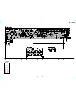
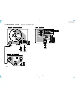
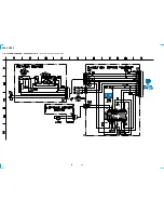
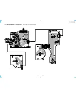
Page 18: ...SCD C333ES 18 18 4 2 SCHEMATIC DIAGRAM RF SECTION Refer to page 40 for Waveforms ...
Page 28: ...SCD C333ES 28 28 4 12 SCHEMATIC DIAGRAM AUDIO SECTION 2 3 ...
Page 29: ...SCD C333ES 29 29 4 13 SCHEMATIC DIAGRAM AUDIO SECTION 3 3 ...
Page 34: ...SCD C333ES 34 34 4 18 SCHEMATIC DIAGRAM HP SECTION ...
Page 36: ...SCD C333ES 36 36 4 20 SCHEMATIC DIAGRAM SENSOR SECTION Refer to page 45 for IC Block Diagram ...
Page 38: ...SCD C333ES 38 38 4 22 SCHEMATIC DIAGRAM POWER SECTION ...

