background image

55

FOCUS command (2X): Focus related. (All servos must be already turned on (except command 21))

No.

Name

Description

Remarks

21

FSRCH ON/OFF

The continuous vertical motion of the optical pick-up lens is turned on or

Avoid a long-time use

off

22

F-BIAS UP

Increase focus bias

Focus bias value

23

F-BIAS DOWN

Decrease focus bias

Focus bias value

24

ADJ FCSBIAS

The focus bias is adjusted automatically
Both + and - directions are searched to search for best jitter point

25

FGAIN UP/DW

The focus servo gain is switched between normal and down

Normal or down are switched alternately

26

FJMP UP/DWN

Focus jump is executed

Valid only for DL

UP: layer 0

t

1, DOWN: layer 1

t

0

27

FOCUS AGC

The focus servo gain is adjusted automatically

28

DISP FBdata

The focus bias adjusted value is displayed

Hexadecimal display 9 bit data

Note:

On or off and up or down are switched alternately

OFFSET (PI, FE, TE) command (3X): Adjusts the offset of PI, FE and TE signals.

No.

Name

Description

Remarks

31

PI/FE OFSET

Adjusts the offset of PI, FE and TE signals

TE offset adjustment is executed for the CD

This adjustment must be executed after 61 DISC DETECT

only

TRACKING command (4X): Tracking servo related.

No.

Name

Description

Remarks

41

TGAIN NM/UP

The tracking servo gain is switched between normal and up

Normal or up are switched alternately

44

ADJ TRK DSP

The traverse AGC and E-F balance adjustment is performed

45

TRACKING AGC

The tracking servo gain is adjusted automatically

SEARCH command (5X): Track search related.(Not used for the servicing)

No.

Name

Description

Remarks

51

1-TRCK JUMP

One-track jump is performed

52

M-TRCK MOVE

M-track movement is performed

53

FINE SEARCH

Fine search is performed

58

CDM Check

Measurement of table rotation hours, tray open/close hours and panel door
open close hours

59

Table Init

Initializes the table.

After this command, the 

[OPEN/CLOSE]

key is enabled.

DISC DETECT command (6X): Disc type check related.

No.

Name

Description

Remarks

61

DISC DETECT

Disc type check is executed

Refer to how to apply servo by manual

Display after judgment

operation (62 page)

DSKMOD CD: Judged as CD
DSKMOD SL: Judged as SACD (SL)
DSKMOD DL: Judged as SACD (DL)
DSKMOD HLHD: Judged as HYBRID HD
DSKMOD CDRW: Judged as CD-RW

62

SET DISC CD

Enter disc type    CD setting

CD forced setting

63

SET DISC SL

Enter disc type    SL setting

SL forced setting

64

SET DISC DD

Enter disc type    DD setting

DD forced setting

65

SET DISC HH

Enter disc type    HYBRID HD setting

HD forced setting

66

SET DISC HC

Enter disc type    HYBRID CD setting

CD forced setting

Summary of Contents for SCD-C333ES - Super Audio Cd Changer

Page 1: ...ignals of the CD General Laser radiant power 5 47 uW at 650 nm These output is the value measured at a distance of about 200mm from the objective lens surface on the optical pick up Power requirements 120 V AC 60 Hz Power consumption 28 W Dimensions w h d 430 138 409 mm 17 5 1 2 16 1 8 in incl projecting parts Mass approx 10 5 kg 23 lbs 3 oz Supplied accessories Design and specifications are subje...

Page 2: ... digital multimeters that have a 2V AC range are suitable See Fig A Fig A Using an AC voltmeter to check AC leakage 0 15µF To Exposed Metal Parts on Set 1 5kΩ AC voltmeter 0 75V Earth Ground TABLE OF CONTENTS 1 SERVICING NOTES 1 3 2 GENERAL 4 3 DISASSEMBLY 3 1 Cover 6 3 2 Front Panel Section 6 3 3 Main Board 7 3 4 Audio Board 7 3 5 CD Mechanism Deck CDM59 DVBU5 8 3 6 Optical Pick Up Block KHM 230A...

Page 3: ...R PRODUCT MARKING is located on the rear exterior SECTION 1 SERVICING NOTES 1 NOTES ON HANDLINGTHE OPTICAL PICK UP BLOCK OR BASE UNIT The laser diode in the optical pick up block may suffer electrostatic break down because of the potential difference generated by the charged electrostatic load etc on clothing and the human body During repair pay attention to electrostatic break down and also use t...

Page 4: ...eceding track when you turn the lAMSL dial clockwise by one click you go to the succeeding track qs CLEAR button 20 Press to delete a programmed track number qd DISC SKIP button 11 Press to select the disc qf PHONE LEVEL control Adjust the headphones volume qg PHONES jack Connect the headphones qh A OPEN CLOSE button 11 Press to open close the disc tray qj Disc tray 11 Press A OPEN CLOSE to open c...

Page 5: ... the track the total remaining time on the disc or TEXT information appears in the display Press to insert a space qg ENTER button 23 Press to decide the selection qh CLEAR button 19 Press to delete a programmed track number qj CHECK button 19 Press to check the programmed order qk SACD CD button 10 Each time you press the button while the Hybrid disc page 11 is loaded the layer changes between an...

Page 6: ...the numerical order given 3 1 COVER 3 2 FRONT PANEL SECTION 3 cover 2 screw TP 1 two screws TP 1 two screws TP 4 two screws BVTP3 8 5 two screws BVTP3 10 6 two screws BVTP3 8 7 screw BVTP3 8 8 front panel section 3 connector CN303 2 connector CN404 1 connector CN906 ...

Page 7: ... two screws BVTP3 8 3 two screws BVTP3 8 4 AUDIO board 7 two screws BVTP3 8 8 two screws BVTP3 8 9 MAIN board 2 wire flat type 35 core CN503 4 wire flat type 16 core CN901 5 wire flat type 8 core CN902 3 connectors CN904 6 connectors CN905 1 connectors CN701 ...

Page 8: ...rews BVTP3 8 3 sub chassis 1 five screws BVTP3 8 4 three screws BVTP3 8 6 screw BVTP3 8 5 Slide the tray until the screw that fixes the table assy can be seen through around hole in the table assy a 7 screw BVTP3 8 8 CD mechanism deck CDM59 DVBU5 ...

Page 9: ...gear U D b b 6 connector CN002 7 three screws BVTP3 8 8 RF board 3 7 TABLE ASSY Note When installing the table assy on the chassis assy engage the gear loading C with the groove by looking into the gear through a hole in the table assy qa table assy 9 three screws BTTP M2 6 e c c d d e 0 bracket guide gear loading C 7 two screws BTTP M2 6 5 screw BTTP M2 6 6 bracket guide 2 two screws BTTP M2 6 1 ...

Page 10: ...NG MOTOR BOARD 3 8 TRAY SENSOR BOARD 1 screw PTPWH M2 6 3 belt rotary 4 two screws BTTP M2 6 4 two screws BTTP M2 6 5 SENSOR board 2 tray 3 two screws BTTP M2 6 4 LOADING MOTOR board 1 belt loading 2 connector CN13 ...

Page 11: ...to the position showing in the Fig A 6 screw PTPWH M2 6 5 stopper washer FR 4 Push fully the shaft of shaft gear and align the hole shape of gear loading B 3 Let the swing gear through under the chassis and engage its dowel with the groove of rotary encoder 2 Install the rotary encoder so that its groove comes to the position shown in the figure 1 Insert the shaft gear up to the position where its...

Page 12: ...ible resistor U B Line V B Line Voltages and waveforms are dc with respect to ground under no signal conditions no mark CD PLAY Voltages are taken with a VOM Input impedance 10 MΩ Voltage variations may be noted due to normal produc tion tolerances Waveforms are taken with a oscilloscope Voltage variations may be noted due to normal produc tion tolerances Circled numbers refer to waveforms Signal ...

Page 13: ... DIN 26 LDON LDON 16 15 14 13 CD_A CD_B CD_C CD_D 6 5 DOOR MOTOR DRIVE MUTE1 M 2 LOAD LOAD DOOR MOTOR 22 IC001 SACD CD RF AMP FOCUS TRACKING ERROR AMP 16 Q003 CD LD DRIVE 21 23 LASER DIODE DVDLD DVDPD DVD_LD DVD_PD Q001 SACD LD DRIVE IC081 6 7 2 1 RFSIN VMOD IC512 SPINDLE DOOR MOTOR DRIVE M1000 17 18 SSTP LIM_SW MUTE_2D SP_ON MUTE_LOAD SPDA SPIN LOAD Q002 Q005 VMOD IC004 2 2 5 7 10 12 8 14 1 65V A...

Page 14: ...49 44 41 39 35 32 30 27 24 79 80 82 87 89 91 IC300 COUNTER IC811 CLOCK Signal Path SACD N M C IC704 SW 1 2 4 SP_DW SP_DW 66 69 71 73 75 96 97 99 101 102 104 106 8 XRST_DVD XHRD XHWR XCS1882 XINIT0 XINIT1 XRST XRD XWR XCS XINT0 XINT1 SCOR MDIN GSCOR EXCK SBSO WFCK C2PO BCLK MDAT LRCK MDP SPIN IC708 2 2 IC708 1 2 IC703 1 2 GFS_V JIT APDO RF_AD_CE WMPLCK SCOR MDIN2 SPO GSCOR EXCK WFCK SBIN C2PO BCLK ...

Page 15: ...D RXD RST INIT_DF LATCH_DF SHIFT_DF SCDATA_DF MODE_DF AMUTE BUSY_DP SDIN SDOUT SLK REQ MUTE_DSD XMSLAT SCK_DSD SDOUT_DSD SDIN_DSD READY_DSD EEP_SIO EEP_SCL T_SENS A1IN XHRD XHWR XCS1882 XINIT0 XINIT1 XCS2 XCS_IO XDIS_IO TXD RXD INIT LATCH SHIFT DATA MODE AMUTE IFBUSY SIN1 IFSOO IFSCO XIFCS SHRMUT XMSLAT MSCK MSDATI MSDATO SHRRDY IC903 EEPROM SDA SCL T_SENS IC909 DECODER A7 XCS2 XHWR IC907 D FF D0 ...

Page 16: ... MODE IN2 IN2 IN1 IN1 I01 I02 I01 I02 IC100 CURRENT PULSE D A IC200 CURRENT PULSE D A IC101 I V CONVERSION IC102 1 2 AUDIO FILTER IC102 2 2 BUFFER RY350 IC307 1 2 HEADPHONE AMP IN2 IO1 IO2 IO1 IO2 IN2 IN1 IN1 IC201 I V CONVERSION IC202 1 2 AUDIO FILTER IC202 2 2 BUFFER IC307 2 2 HEAD PHONE AMP R L DATAI BCKI LRCKI SDATA L SDATA R SBCKI INIT NREGCLR LATCH SHIFT SCDATA MODE LVCK02 L1 L1 L2 L2 R2 R2 ...

Page 17: ...000 FLUORESCENT INDICATOR TUBE 43 KEY 1 44 KEY 2 45 KEY 3 16 D410 413 D422 425 12V REG 2 3 IC404 T902 POWER TRANSFORMER D414 417 D402 405 F1 F2 T901 POWER TRANSFORMER Q401 31V REG D406 409 AC IN S1003 1005 1007 1010 1011 S1000 1 2 1012 1014 1016 1018 1020 S1013 1015 1017 1019 1021 LED DRIVER S1000 1 2 SACD CD Q1004 LED DRIVER D1000 Q1005 LED DRIVER D1001 Q1006 LED PAUSE LED PLAY LED SACD CD 31V VF...

Page 18: ...SCD C333ES 18 18 4 2 SCHEMATIC DIAGRAM RF SECTION Refer to page 40 for Waveforms ...

Page 19: ...r to page 12 for Circuit Board Location Page 20 Ref No Location D001 A 1 D002 B 3 IC001 E 3 IC004 F 4 IC081 C 5 Q001 B 2 Q002 C 3 Q003 B 3 Q005 B 2 Semiconductor Location There are a few cases that the part printed on this diagram isn t mounted in this model ...

Page 20: ...at the part printed on this diagram isn t mounted in this model Page 33 Page 35 Page 37 Page 30 Page 30 Page 30 Page 19 Page 30 Page 30 Ref No Location D901 C 5 D902 C 5 D903 I 11 IC509 F 6 IC701 F 10 IC704 G 9 IC801 B 10 IC803 D 8 IC804 C 8 IC901 B 3 IC902 C 6 IC905 D 5 IC907 B 5 IC909 B 5 Q901 C 5 Q905 C 5 Semiconductor Location ...

Page 21: ...is diagram isn t mounted in this model Ref No Location D904 G 2 IC502 D 9 IC503 D 5 IC504 E 11 IC512 D 11 IC703 C 2 IC706 D 2 IC708 D 5 IC805 G 5 IC806 C 1 IC807 C 1 IC808 G 3 IC809 G 1 IC810 H 2 IC811 C 2 IC812 G 4 IC813 H 3 IC814 H 3 IC815 I 3 IC903 I 7 IC904 F 11 IC906 G 11 IC908 G 8 IC910 G 4 IC920 I 6 Q902 H 5 Q903 H 6 Q904 H 6 Semiconductor Location ...

Page 22: ...SCD C333ES 22 22 4 6 SCHEMATIC DIAGRAM MAIN SECTION 1 5 Refer to page 49 for IC Pin Function PIN FUNCTION ...

Page 23: ...SCD C333ES 23 23 4 7 SCHEMATIC DIAGRAM MAIN SECTION 2 5 Refer to page 40 for Waveforms Refer to page 41 for IC Block Diagrams Refer to page 46 for IC Pin Function PIN FUNCTION ...

Page 24: ...SCD C333ES 24 24 4 8 SCHEMATIC DIAGRAM MAIN SECTION 3 5 Refer to page 40 for Waveform Refer to page 41 for IC Block Diagrams Refer to page 48 for IC Pin Function PIN FUNCTION ...

Page 25: ...SCD C333ES 25 25 4 9 SCHEMATIC DIAGRAM MAIN SECTION 4 5 Refer to page 40 for Waveform Refer to page 42 for IC Block Diagrams ...

Page 26: ...SCD C333ES 26 26 4 10 SCHEMATIC DIAGRAM MAIN SECTION 5 5 Refer to page 40 for Waveform Refer to page 43 for IC Block Diagrams ...

Page 27: ...SCD C333ES 27 27 4 11 SCHEMATIC DIAGRAM AUDIO SECTION 1 3 Refer to page 40 for Waveforms Refer to page 44 45 for IC Block Diagrams ...

Page 28: ...SCD C333ES 28 28 4 12 SCHEMATIC DIAGRAM AUDIO SECTION 2 3 ...

Page 29: ...SCD C333ES 29 29 4 13 SCHEMATIC DIAGRAM AUDIO SECTION 3 3 ...

Page 30: ...D406 D 2 D407 D 2 D408 D 2 D409 D 2 D410 D 1 D411 D 1 D412 D 1 D413 D 1 D414 E 3 D415 E 3 D416 E 3 D417 E 3 D418 G 8 D419 F 8 D422 F 4 D423 F 4 D424 F 4 D425 F 4 D426 E 4 D427 B 2 D428 B 3 D432 F 1 D433 F 1 D434 F 1 IC100 B 7 IC101 C 10 IC102 C 12 IC200 D 7 IC201 Q 9 IC202 F 11 IC300 D 4 IC301 D 5 IC302 C 6 IC303 B 4 IC304 C 8 IC305 D 8 IC306 B 9 IC307 G 12 IC385 D 13 IC400 B 3 IC401 B 1 IC402 C 1...

Page 31: ...SCD C333ES 31 31 4 15 PRINTED WIRING BOARD AUDIO SECTION SIDE B Refer to page 12 for Circuit Board Location ...

Page 32: ...SCD C333ES 32 32 4 16 SCHEMATIC DIAGRAM DISPLAY SECTION Refer to page 45 for IC Block Diagrams ...

Page 33: ...ISPLAY SECTION Refer to page 12 for Circuit Board Location Page 20 Page 35 Page 30 Ref No Location D1000 A 5 D1001 A 4 D1002 B 4 D1003 B 12 IC1001 B 9 IC1002 B 6 Q1000 B 8 Q1001 B 9 Q1002 B 7 Q1004 B 12 Q1005 A 5 Q1006 A 5 Semiconductor Location ...

Page 34: ...SCD C333ES 34 34 4 18 SCHEMATIC DIAGRAM HP SECTION ...

Page 35: ...SCD C333ES 35 35 4 19 PRINTED WIRING BOARD HP SECTION Refer to page 12 for Circuit Board Location Page 33 Page 20 Page 30 ...

Page 36: ...SCD C333ES 36 36 4 20 SCHEMATIC DIAGRAM SENSOR SECTION Refer to page 45 for IC Block Diagram ...

Page 37: ...SCD C333ES 37 37 4 21 PRINTED WIRING BOARD SENSOR SECTION Refer to page 12 for Circuit Board Location 16 TO MAIN BOARD Page 20 ...

Page 38: ...SCD C333ES 38 38 4 22 SCHEMATIC DIAGRAM POWER SECTION ...

Page 39: ...SCD C333ES 39 39 4 23 PRINTED WIRING BOARD POWER SECTION Refer to page 12 for Circuit Board Location Page 30 Page 30 Page 30 ...
Page 40: ...s 7 IC801 rh BCKA 2 IC809 8 X2Q 6 IC801 rs BCKD 3 IC809 qa 2CK 4 IC811 1 2 1 Vp p 88 5 ns 3 8 Vp p 177 ns 3 7 Vp p 354 ns 3 1 Vp p 177 ns 3 4 Vp p 354 ns 9 IC801 qf MCKI 8 IC509 t RFAC CD PLAY 2 IC301 rf LVCKO2 IC300 1 CLK 3 IC301 rl BCKI AUDIO Board 1 IC300 5 Q 4 IC301 t LRCKI 5 IC301 ta SBCKI 2 9 Vp p 29 5 ns Approx 1 4 Vp p 3 2 Vp p 88 5 ns 3 4 Vp p 354 ns 3 5 Vp p 22 7 µs 3 4 Vp p 354 ns 4 4 V...
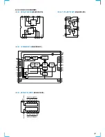
Page 41: ...ONTROL INPUT DATA BUFFER OUTPUT DATA BUFFER ADDRESS BUFFER ROW DECODER MEMORY CELL ARRAY 512 x 512 OE A11 A9 A8 A13 VCC A14 A12 A7 A6 A5 A4 A3 WE A2 A1 A0 I O1 I O2 I O3 GND I O4 I O5 I O6 I O7 I O8 A10 CE 8 15 16 10 14 13 12 11 G A B Y0 Y1 Y2 Y3 9 6 7 4 5 2 3 1 G A B Y0 Y1 Y2 Y3 VCC 2G ENABLE 2Y0 2Y1 2Y2 2Y3 2A 2B 1Y0 1Y1 1Y2 1Y3 1A 1B GND 1G ENABLE SELECT DATA OUTPUTS SELECT DATA OUTPUTS IC809 S...
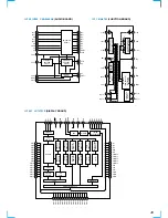
Page 42: ...D A CONV 8bit R 2R D A CONV 8bit LATCH 8bit LATCH D0 1 2 3 4 5 6 D7 D8 9 10 D11 12bit SHIFT REGISTER ADD DECODER D A D A L L D A L D A L D A L D A L D A L D A D A D A L L L Ch3 4 5 6 7 8 9 10 Ch2 1 12 11 VSS VrefL VDD VrefH VCC D0 A03 A04 A05 A06 A07 A08 A09 A010 A011 A012 LD CLK DI A01 A02 GND ...
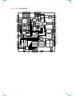
Page 43: ...S CLOK XLAT DATA MUTE SCLK GFS C4M 63 62 61 60 59 58 57 56 55 54 53 52 51 50 49 48 65 64 47 46 45 44 43 42 41 LRCK DOUT VPC0 ASYE MD2 FIL0 CLTV ASY0 ASY1 RFAC AVSS1 FIL1 PCO DVDD2 BIAS V16M CE TE RFDC AD10 AVSS0 1GEN AVDD CLOCK GENERATOR ASYMMETY CORRECTOR DIGITAL PLL EFM DEMODURATOR DIGITAL PLL CPU INTERFACE SERVO AUTO SEQUENCER SERVO INTERFACE SUB CODE PROCESSOR DIGITAL OUT ERROR CORRECTOR 32K R...

Page 44: ... 21 22 23 24 128FSO INVI INVO VSS VSS DATAI BCKI LRCKI SBCKI SDATAR SDATAL DATAVD VDD DRPOL MTPOL PWMSEL MUTER MUTEL VSS NSCKSEL DFCKSEL CKTL3 R1 NSDOR4 R1 NSDOR3 R2 NSDOR2 R2 NSDOR1 VsubR1 AVDDR1 AVDDR2 VsubR2 VSSR2 VsubX XVSS XIN XOUT XVDD 64FSI VSSL2 AVDDL2 AVDDL1 VsubL1 VsubL2 L1 NSDOL4 L2 NSDOL2 L2 NSDOL1 L1 NSDOL3 LVCKO2 LVCKO1 CKTL2 CKTL1 CKTL0 TEST2 TEST1 DFIOSEL DFLRCK DFDTL DFDTR DFBCK D...

Page 45: ... 44 AA8 G12 43 AA7 G13 42 AA6 G14 41 AA5 G15 40 AA4 G16 39 AA3 38 AA2 37 AA1 36 AM35 35 AM34 34 AM33 33 63 CL 62 CE 64 DI 61 60 VDD 59 OSCI 58 OSCO 57 VSS 56 TEST 55 VFL G1 54 G2 53 G3 52 G4 51 G5 50 G6 49 RES DECODER SHIFT REGISTER DC RAM LATCH CG RAM CG ROM AD RAM LATCH ANODE GRID DRIVER ADDRESS COUNTER BLINK GENERATOR DISPLAY CONTROL DUTY GENERATOR CONTROL TIMING GENERATOR DIVIDER OSC ADDRESS R...

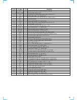
Page 46: ...ut output terminal 44 1kHz Not used open 20 NC Not used open 21 MNT2 O Monitor 2 signal output terminal Not used open 22 TRST I Reset signal input terminal normally fixed at L 23 TCK I Clock signal input terminal for test normally fixed at L 24 TDI I Data input terminal for test normally open 25 TENA1 I Data enable signal input terminal for test normally open 26 TDO O Data output terminal for test...

Page 47: ...ddress strobe signal output to the D RAM IC808 69 XOE O Read enable signal output to the D RAM IC808 70 to77 DQ0 to DR7 I O Two way data bus with the D RAM IC808 78 VDD Power supply terminal 3 3V 79 VSS Ground terminal 80 WCK I Clock signal input terminal for disk mark detect 81 WRFD I RF data signal input terminal for disk mark detect 82 to 89 WAD0 to WAD7 I A D data signal input from the A D con...

Page 48: ...set Signal for CD DSP Ground terminal Power supply terminal MULTI 2CH SW for AUDIO board 1 MULTI RF amplifier serial enable signal SEN_RF To be used for disc inspection mode Data bus Data bus Not used open Data bus Clear signal input terminal Pull up Reset signal input from the ARP Ground terminal Strobe signal input from the CPU Strobe signal input from the CPU Chip enable signal input from the C...

Page 49: ...gital system Not used open Stream data signal output to the DSD decoder IC801 Not used open Stream data signal output to the DSD decoder IC801 Ground terminal digital system Not used open Stream data signal output to the DSD decoder IC801 Power supply terminal 3 3V digital system Not used open Power supply terminal 5V digital system Stream data signal output to the DSD decoder IC801 Not used open ...

Page 50: ... Ground terminal digital system Address signal output to the D RAM IC706 RF data signal output terminal for disc mark detection Clock signal output terminal for disc mark detection Monitor signal output to the CPU IC901 Output enable signal output to the D RAM IC706 Column address strobe signal output to the D RAM IC706 Two way data bus with the D RAM IC706 Ground terminal digital system Two way d...

Page 51: ...bcode sync OR signal input from the CXD3008Q IC509 Subcode serial data reading clock signal output to the CXD3008Q IC509 Subcode serial data input from the CXD3008Q IC509 Ground terminal digital system Subcode sync OR signal input from the CXD3008Q IC509 Write frame clock signal input from the CXD3008Q IC509 Power supply terminal 5V RAM overflow signal input terminal Not used fixed at L Power supp...

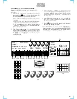
Page 52: ...ror signal offset auto adjustment 5 Spindle kick for LD on 6 LD on 7 Focus search 8 Focus servo on 9 Spindle kick 10 Spindle servo on 11 E F balance auto adjustment 12 Tracking sled servo on 13 Focus bias auto adjustment 14 Focus servo gain auto adjustment 15 Tracking servo gain auto adjustment 16 Jump to lead in area 17 Read TOC 18 Auto play track No 1 SECTION 5 SERVICING NOTES 2 3 SACD dual laye...

Page 53: ...lockwise to turn on the calendar segments sequentially When the segment 15 is confirmed turn JOG counter clockwise that turns off the calendar segment When the segment 1 is confirmed this is the end of check 4 After all the checks are completed confirm to see that the dis play TEST END appears The message indicates that the check is ended normally 5 Press the button to turn off the main power and ...

Page 54: ...e 1 Category Application SATD 04 12 cm disc Adjusted value check J 2501 184 A SL Reference disc Operation check Optical waveform check Not specified DL 12 cm disc Operation check PATD 012 Adjusted value check 4 225 203 01 CD 12 cm disc Operation check YEDS 18 Reference disc Optical waveform check 3 702 101 01 Not specified HYBRID 12 cm disc Operation check 1 SL Single Layer DL Dual Layer Setting M...

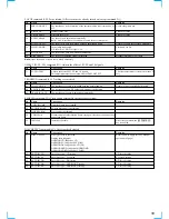
Page 55: ...rvo related No Name Description Remarks 41 TGAIN NM UP The tracking servo gain is switched between normal and up Normal or up are switched alternately 44 ADJ TRK DSP The traverse AGC and E F balance adjustment is performed 45 TRACKING AGC The tracking servo gain is adjusted automatically SEARCH command 5X Track search related Not used for the servicing No Name Description Remarks 51 1 TRCK JUMP On...

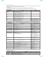
Page 56: ...95 DISPLAY ERROR The content of error recorded to the set is read and displayed Error recording Only one item is recorded 96 D OUT OnOff Digital out of CD is turned on or off Not used in this set 98 APDO JITTER Not used for the servicing 9C BU DENCHO The content of error recorded to the set is read and then the S curve Refer to 6 8 WAVEFORMS CHECK waveform traverse waveform and RF waveform can be ...

Page 57: ... press the AMS dial to enter 3 When 10 TOTAL CHECK is displayed rotate the AMS dial clockwise by 2 clicks to select 12 MANUAL CHK and press the AMS dial to enter 4 When 120 MANUAL CHK is displayed rotate the AMS dial clockwise by 4 clicks to select 124 READ TOC PSP and press the AMS dial to enter 5 A checking will start automatically Note In making a check the disc must be loaded Immediately when ...

Page 58: ...e address line WE etc 4 D903 1SS367 is faulty CD DSP ERROR 1 IC509 CD DSP is faulty 2 768fs 33 86688 MHz is not present to IC509 pin ua XTAL Same as cause 3 of DVD DEC ERROR 3 IC509 pin 2 XRST does not go H IC901 pin rf XDIS does not go H IC902 expander is faulty D A ERROR 1 IC904 D A converter is faulty 2 Faulty IC703 jitter amplifier peripheral circuits 3 IC901 pin yf JIT is faulty EEPROM ERROR ...

Page 59: ... RF 8 bit data in hex notation RF A0h VC FE TE 9 bit data in hex notation VC FE TE 00h RF VC FE TE ADJ Offset values after RF PI VC FE TE signal offset adjustment VC offset is not adjusted Less than ORG value if offset correction is normal Measurement only RF 8 bit data in hex notation Also for SACD the TE offset is VC FE TE 9 bit data in hex notation not measured and adjusted PI TRVS PP ORG ADJ P...

Page 60: ...surement was taken place Specified Value 1 SACD Use the test disc SATD S4 Note Measured values in check items are typical ones Check items Specified value LOAD IN TIME msec Not displayed in this set SPIN UP TIME msec 1652 2000 msec or less RF VC FE TE AVRG ORG 98 C 1DE 0 RF 80 9B VC 1F1 10 FE 1d8 42 TE 1BB 5C RF VC FE TE AVRG ADJ 9F C 4 0 RF 98 A5 VC 1F1 10 FE 1F1 10 TE 1F1 10 PI TRVS PP ORG ADJ 8...

Page 61: ... MIN MAX msec 850 833 860 AVE 1100 msec or less MAX 1400 msec or less 1 MAX SEEK TIME F AVE MIN MAX msec 2086 1999 2151 AVE 2400 msec or less MAX 2800 msec or less R AVE MIN MAX msec 1805 1793 1835 AVE 2400 msec or less MAX 2800 msec or less ERROR RATE C1 MAX AVE 3 0 C1 MAX 30 or less C2 MAX AVE 0 0 C2 MAX 0 HENSHIN RYOU 1 10um 89 1000 or less 100 um or less SPIN DOWN TIME msec 1272 1700 msec or l...

Page 62: ...of 5 allows the check ing to be repeated by the set number of times Also setting 0 zero allows the aging check to be repeated until an error oc curs 6 4 HYBRID DISC OPERATION CHECK Perform as necessary This test checks the auto adjustment time required when the disc is switched between HD SACD layer and CD layer This test is conducted to check the stability in switching from CD to SACD or SACD to ...

Page 63: ...dure 1 Enter the TEST mode Turn the AMS dial and select 59 Table Init Press AMS once that enables the OPEN CLOSE key 2 When the message INITIAL OK appears press the OPEN CLOSE key to eject the tray Place a disc in the DISC1 of the table Be sure to place a disc in DISC1 If a disc is placed in any locations other than DISC1 the correct measurement can not be executed Therefore be sure to place a dis...

Page 64: ...P key turn the AMS dial and then press the CONTINUE key The program does not ad vance if these keys are not pressed in the above sequence 3 The panel door repeats opening and closing 4 The messages AP B 000000 during open t AP C 000000 during close are repeated on the FL display Num ber of times of open close are displayed in decimal number in 000000 with OPEN CLOSE as a set 5 Press the STOP key t...

Page 65: ...n of display An error code is displayed in From From 1 means retry failed 3 times From 2 means abnormal value Optical pick up RF amplifier or CD DSP IC is faulty FCS AGC ERROR Error at focus gain automatic adjustment Defocusing during adjustment Optical pick up RF amplifier or CD DSP IC is faulty TRK AGC ERROR Error at tracking gain automatic adjustment Defocusing during adjustment Optical pick up...

Page 66: ...ill be displayed for PATD 012 or YEDS 18 Note For the SATD S4 SACD DETECT is displayed 3 Press again the AMS dial and the S curve waveform check mode will become active and S J1 MODE will be displayed 4 Connect an oscilloscope to the TP506 FE and TP504 AVC on the MAIN board 5 Check that the level A and B of waveform on the oscilloscope satisfy the specification Specified Value Disc A B SATD 04 PAT...

Page 67: ...ved in the center Checking and Connecting Location See page 68 MAIN board TP703 RFAC TP704 AGND oscilloscope VOLT DIV 200 mV TIME DIV 500 ns RF signal waveform A CLV Jitter Check CD only Connection Checking Method 1 Set the test mode 2 Connect an oscilloscope to the TP516 RFCK CH1 TP517 WFCK CH2 and TP808 DG GND on the MAIN board 3 Place the test disc PATD 012 or YEDS 18 on the tray and close the ...

Page 68: ...68 Checking and Connecting Location MAIN Board Component Side TP513 TE TP504 AVC TP506 FE TP517 WFCK TP516 RFCK TP808 DG IC801 IC701 IC509 TP703 RFAC TP704 AGND ...

Page 69: ...ark list and accessories and packing materials are given in the last of this parts list 69 The components identified by mark 0 or dotted line with mark 0 are critical for safety Replace only with part number specified Les composants identifiés par une marque 0 sont critiques pour la sécurité Ne les remplacer que par une pièce portant le numéro spécifié 7 1 CASE SECTION Ref No Part No Description R...

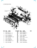
Page 70: ...714 01 EMBLEM SACD 57 4 992 539 11 KNOB PHONE LEVEL 58 4 230 720 01 ESCUTCHEON H P 59 4 230 636 11 PLATE REMOTE INDICATION 60 4 230 637 11 KNOB AMS 61 4 230 717 01 PANEL FRONT 62 4 230 709 01 SPRING SHAFT L 63 4 220 711 01 INDICATOR FILTER 64 4 230 721 01 WINDOW FL 65 4 230 638 01 INDICATOR BUTTON PLAY 66 4 923 520 01 KNOB POWER 67 4 220 319 11 BUTTON MODE 68 4 220 317 01 BUTTON FILTER 69 4 230 72...

Page 71: ... 11 WIRE FLAT TYPE 35 CORE 103 1 757 136 11 WIRE FLAT TYPE 16 CORE 104 1 757 137 11 WIRE FLAT TYPE 9 CORE 105 4 966 267 12 BUSHING FBS001 CORD 0106 1 783 531 31 CORD POWER 107 4 230 686 01 PANEL BACK 108 X 4945 356 3 FOOT ASSY F50180S 0T101 1 435 732 11 TRANSFORMER POWER 0T102 1 435 733 11 TRANSFORMER POWER Note The components identified by mark 0 or dotted line with mark 0 are critical for safety...

Page 72: ...d not supplied 204 M11 201 206 203 202 202 203 not supplied 201 4 224 603 01 TRAY 202 4 218 253 01 SCREW M2 6 BTTP 203 4 224 619 01 BRACKET GUIDE 204 4 224 602 01 TABLE 205 4 224 617 01 GEAR RM E 206 4 985 672 01 SCREW PTPWHM2 6 FLOATING 207 4 224 616 01 GEAR RM M 208 4 224 615 01 GEAR RM B 209 4 225 328 01 BELT ROTARY 210 1 676 245 11 SENSOR BOARD M11 A 4672 867 A MOTOR ASSY ROTARY TRAY ...

Page 73: ... 224 611 01 GEAR LOADING B 263 3 016 533 21 WASHER FR STOPPER 264 4 951 619 21 CUSHION A 265 4 224 606 01 GEAR RV 266 4 224 605 01 GEAR U D 267 X 4953 250 1 PLATE A ASSY CHUCKING 268 3 061 886 01 YOKE 269 4 229 957 01 PLATE B CHUCKING 270 4 224 618 01 LEVER LIFTER 271 1 791 930 11 WIRE FLAT TYPE 6 CORE 272 4 227 549 11 INSULATOR 273 1 757 097 11 WIRE FLAT TYPE 25 CORE 274 4 951 620 01 SCREW 2 6X8 ...

Page 74: ... 165 319 11 CERAMIC CHIP 0 1uF 50V C101 1 136 850 11 MYLAR 0 1uF 5 00 63V C102 1 165 319 11 CERAMIC CHIP 0 1uF 50V C103 1 128 654 21 FILM 2200PF 5 50V C105 1 163 141 00 CERAMIC CHIP 0 001uF 5 50V C106 1 109 857 11 ELECT 47uF 20 00 63V C107 1 136 850 11 MYLAR 0 1uF 5 00 63V C108 1 163 141 00 CERAMIC CHIP 0 001uF 5 50V C109 1 130 955 00 FILM 0 01uF 5 00 100V C110 1 130 955 00 FILM 0 01uF 5 00 100V C...

Page 75: ...342 1 164 695 11 CERAMIC CHIP 0 0022uF 5 00 50V C344 1 164 695 11 CERAMIC CHIP 0 0022uF 5 00 50V C345 1 124 927 11 ELECT 4 7uF 20 100V C346 1 163 133 00 CERAMIC CHIP 470PF 5 50V C347 1 164 695 11 CERAMIC CHIP 0 0022uF 5 00 50V C348 1 164 695 11 CERAMIC CHIP 0 0022uF 5 00 50V C349 1 164 695 11 CERAMIC CHIP 0 0022uF 5 00 50V C350 1 165 319 11 CERAMIC CHIP 0 1uF 50V C351 1 164 695 11 CERAMIC CHIP 0 0...

Page 76: ... 210 39 DIODE EC10QS04 TE12L5 D425 8 719 210 39 DIODE EC10QS04 TE12L5 D426 8 719 210 39 DIODE EC10QS04 TE12L5 D427 8 719 210 39 DIODE EC10QS04 TE12L5 D428 8 719 210 39 DIODE EC10QS04 TE12L5 D432 8 719 820 05 DIODE 1SS181 TE85L D433 8 719 801 78 DIODE 1SS184 TE85L D434 8 719 158 49 DIODE UDZ TE 17 12B IC IC100 8 759 371 51 IC CXA8042AS IC101 8 759 566 39 IC OPA2132UA 2K5 IC102 8 759 566 39 IC OPA21...

Page 77: ...99 11 CARBON MELF 2 2K 2 1 8W R220 1 260 002 11 CARBON MELF 3 3K 2 1 8W R221 1 260 002 11 CARBON MELF 3 3K 2 1 8W R222 1 260 002 11 CARBON MELF 3 3K 2 1 8W R223 1 259 971 11 CARBON MELF 10 2 1 8W R224 1 259 971 11 CARBON MELF 10 2 1 8W R303 1 216 019 00 METAL CHIP 56 5 1 10W R304 1 216 073 00 METAL CHIP 10K 5 1 10W R305 1 216 073 00 METAL CHIP 10K 5 1 10W R306 1 216 033 00 METAL CHIP 220 5 1 10W R...

Page 78: ...6 1 506 468 11 PIN CONNECTOR 3P DIODE D1000 8 719 046 40 DIODE SEL5521C TH8F D1001 8 719 046 35 DIODE SEL5921A TH8F D1002 8 719 016 74 DIODE 1SS352 TPH3 D1003 8 719 210 39 DIODE EC10QS04 TE12L5 GROUND ET1001 1 537 770 21 TERMINAL BOARD GROUND FILTER FL1000 1 518 715 11 INDICATOR TUBE FLUORESCENT IC IC1001 8 759 337 52 IC LC75721E IC1002 8 752 921 04 IC XP84120 089Q TRANSISTOR Q1000 8 729 900 53 TR...

Page 79: ...CLEAR VIBRATOR X1000 1 781 472 21 VIBRATOR CERAMIC DOOR MOTOR BOARD CAPACITOR C1027 1 165 319 11 CERAMIC CHIP 0 1uF 50V CONNECTOR CN1005 1 568 942 11 PIN CONNECTOR 4P CN1008 1 506 481 11 PIN CONNECTOR 2P DOOR SW BOARD CN1016 1 568 941 11 PIN CONNECTOR 3P SWITCH S1022 1 771 339 41 SWITCH PUSH IN SW S1023 1 771 339 41 SWITCH PUSH OUT SW HP BOARD 4 962 201 01 PLATE HP GROUND CAPACITOR C1101 1 163 141...

Page 80: ...HIP 0 47uF 10 00 10V C543 1 107 826 11 CERAMIC CHIP 0 1uF 10 00 16V C544 1 107 826 11 CERAMIC CHIP 0 1uF 10 00 16V C545 1 125 822 11 TANTALUM 10uF 20 00 10V C547 1 107 826 11 CERAMIC CHIP 0 1uF 10 00 16V C548 1 162 970 11 CERAMIC CHIP 0 01uF 10 25V C549 1 107 826 11 CERAMIC CHIP 0 1uF 10 00 16V C550 1 162 963 11 CERAMIC CHIP 680PF 10 50V C551 1 125 891 11 CERAMIC CHIP 0 47uF 10 00 10V C553 1 162 9...

Page 81: ... 11 CERAMIC CHIP 0 01uF 10 25V C811 1 162 970 11 CERAMIC CHIP 0 01uF 10 25V C812 1 162 970 11 CERAMIC CHIP 0 01uF 10 25V C813 1 162 970 11 CERAMIC CHIP 0 01uF 10 25V C814 1 125 822 11 TANTALUM 10uF 20 00 10V C815 1 162 970 11 CERAMIC CHIP 0 01uF 10 25V C823 1 125 822 11 TANTALUM 10uF 20 00 10V C824 1 164 677 11 CERAMIC CHIP 0 033uF 10 00 16V C825 1 162 970 11 CERAMIC CHIP 0 01uF 10 25V C826 1 125 ...

Page 82: ...ILTER CHIP EMI FL807 1 234 177 21 FILTER CHIP EMI FL808 1 234 177 21 FILTER CHIP EMI FL809 1 234 177 21 FILTER CHIP EMI FL814 1 234 177 21 FILTER CHIP EMI FL901 1 234 177 21 FILTER CHIP EMI FL902 1 234 177 21 FILTER CHIP EMI FL903 1 234 177 21 FILTER CHIP EMI FL904 1 234 177 21 FILTER CHIP EMI FL905 1 234 177 21 FILTER CHIP EMI FL906 1 234 177 21 FILTER CHIP EMI FL907 1 234 177 21 FILTER CHIP EMI ...

Page 83: ...1 16W R605 1 216 864 11 METAL CHIP 0 5 1 16W R606 1 216 841 11 METAL CHIP 47K 5 1 16W R607 1 218 708 11 METAL CHIP 4 7K 0 5 1 16W R608 1 218 716 11 METAL CHIP 10K 0 5 1 16W R609 1 216 864 11 METAL CHIP 0 5 1 16W R610 1 216 864 11 METAL CHIP 0 5 1 16W R611 1 218 724 11 METAL CHIP 22K 0 5 1 16W R612 1 216 864 11 METAL CHIP 0 5 1 16W R613 1 216 857 11 METAL CHIP 1M 5 1 16W R614 1 216 864 11 METAL CHI...

Page 84: ...CHIP 22 5 1 16W R810 1 216 801 11 METAL CHIP 22 5 1 16W R811 1 216 801 11 METAL CHIP 22 5 1 16W R812 1 216 801 11 METAL CHIP 22 5 1 16W R813 1 216 801 11 METAL CHIP 22 5 1 16W R814 1 216 801 11 METAL CHIP 22 5 1 16W R815 1 216 801 11 METAL CHIP 22 5 1 16W R816 1 216 809 11 METAL CHIP 100 5 1 16W R817 1 216 809 11 METAL CHIP 100 5 1 16W R819 1 216 809 11 METAL CHIP 100 5 1 16W R820 1 218 713 11 MET...

Page 85: ... METAL CHIP 10K 5 1 16W R979 1 216 833 11 METAL CHIP 10K 5 1 16W R980 1 216 833 11 METAL CHIP 10K 5 1 16W R981 1 216 833 11 METAL CHIP 10K 5 1 16W R982 1 216 864 11 METAL CHIP 0 5 1 16W R983 1 216 864 11 METAL CHIP 0 5 1 16W R985 1 218 712 11 METAL CHIP 6 8K 0 5 1 16W R988 1 216 864 11 METAL CHIP 0 5 1 16W R991 1 216 864 11 METAL CHIP 0 5 1 16W R992 1 216 864 11 METAL CHIP 0 5 1 16W R994 1 216 789...

Page 86: ...3 8 729 805 25 TRANSISTOR 2SB1121 ST TD Q005 8 729 820 90 TRANSISTOR 2SD1621 ST TD RESISTOR R001 1 216 864 11 METAL CHIP 0 5 1 16W R002 1 218 668 11 METAL CHIP 100 0 5 1 16W R003 1 216 839 11 METAL CHIP 33K 5 1 16W R005 1 216 864 11 METAL CHIP 0 5 1 16W R006 1 216 864 11 METAL CHIP 0 5 1 16W R007 1 216 864 11 METAL CHIP 0 5 1 16W R008 1 216 864 11 METAL CHIP 0 5 1 16W R011 1 216 864 11 METAL CHIP ...

Page 87: ...S200 1 418 746 11 ENCODER ROTARY 0T101 1 435 732 11 TRANSFORMER POWER 0T102 1 435 733 11 TRANSFORMER POWER ACCESSORIES PACKING MATERIALS 1 476 263 11 REMOTECOMMANDER RM SC300 1 558 271 11 CORD CONNECTION 4 230 687 01 MANUAL INSTRUCTION ENGLISH 4 228 696 01 COVER BATTERY for RM SC300 HARDWARE LIST 1 7 685 646 79 SCREW BVTP3X8 TYPE2 N S 2 7 685 871 01 SCREW BVTT3X6 S 4 7 685 885 09 SCREW BVTT4X16 S ...

Page 88: ...88 Sony Corporation Audio Entertainment Group 9 929 551 11 2000J1613 1D Printed in Japan 2000 10 Published by General Engineering Dept SCD C333ES ...

Reviews: