SCD-C333ES
19
19
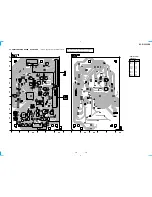
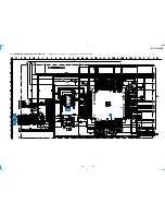
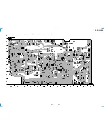
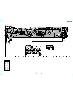
4-3. PRINTED WIRING BOARD RF SECTION
• Refer to page 12 for Circuit Board Location.
(Page 20)
Ref. No.
Location
D001
A-1
D002
B-3
IC001
E-3
IC004
F-4
IC081
C-5
Q001
B-2
Q002
C-3
Q003
B-3
Q005
B-2
• Semiconductor
Location
There are a few cases that the part printed on
this diagram isn’t mounted in this model.
Summary of Contents for SCD-C333ES - Super Audio Cd Changer
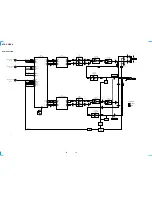
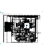
Page 18: ...SCD C333ES 18 18 4 2 SCHEMATIC DIAGRAM RF SECTION Refer to page 40 for Waveforms ...
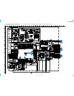
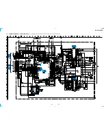
Page 28: ...SCD C333ES 28 28 4 12 SCHEMATIC DIAGRAM AUDIO SECTION 2 3 ...
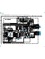
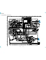
Page 29: ...SCD C333ES 29 29 4 13 SCHEMATIC DIAGRAM AUDIO SECTION 3 3 ...
Page 34: ...SCD C333ES 34 34 4 18 SCHEMATIC DIAGRAM HP SECTION ...
Page 36: ...SCD C333ES 36 36 4 20 SCHEMATIC DIAGRAM SENSOR SECTION Refer to page 45 for IC Block Diagram ...
Page 38: ...SCD C333ES 38 38 4 22 SCHEMATIC DIAGRAM POWER SECTION ...


