background image

SERVICE MANUAL

DCR-TRV6/TRV6E/TRV11/

TRV11E/TRV20/TRV20E

RMT-808/809/811/812

US Model

Canadian Model

Korea Model

DCR-TRV6/TRV11/TRV20

AEP Model

UK Model

Australian Model

Chinese Model

DCR-TRV6E/TRV11E/TRV20E

E Model

Hong Kong Model

Tourist Model

DCR-TRV6/TRV6E/TRV11/

TRV11E/TRV20/TRV20E

SERVICE MANUAL

DIGITAL VIDEO CAMERA RECORDER

J MECHANISM

SPECIFICATIONS

DCR-TRV6/TRV11/TRV20

: NTSC model

DCR-TRV6E/TRV11E/TRV20E : PAL model

For MECHANISM ADJUSTMENTS, refer to the
“DV MECHANICAL ADJUSTMENT MANUAL 
 J MECHANISM  ” (9-929-807-11).

— Continued on next page —

Level 2

On the VC-240/241 board

This service manual provides the information that is premised the
circuit board replacement service and not intended repair inside the
VC-240/241 board.
Therefore, schematic diagram, printed wiring board and electrical parts
list of the VC-240/241 board are not shown.
The following pages are not shown.

Schematic diagram .......................... Pages 4-17 to 4-66
Printed wiring board ......................... Pages 4-67 to 4-74
Electrical parts list ............................ Pages 6-23 to 6-44

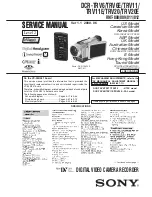
Photo : DCR-TRV20E

RMT-811

• Table showing differences is shown on page 4.

Ver 1.1  2000. 06

Summary of Contents for Handycam DCR-TRV11

Page 1: ...ADJUSTMENTS refer to the DV MECHANICAL ADJUSTMENT MANUAL J MECHANISM 9 929 807 11 Continued on next page Level 2 On the VC 240 241 board This service manual provides the information that is premised the circuit board replacement service and not intended repair inside the VC 240 241 board Therefore schematic diagram printed wiring board and electrical parts list of the VC 240 241 board are not show...

Page 2: ...surface for solder splashes and bridges 2 Check the interboard wiring to ensure that no wires are pinched or contact high wattage resistors 3 Look for unauthorized replacement parts particularly transistors that were installed during a previous repair Point them out to the customer and recommend their replacement 4 Look for parts which through functioning show obvious signs of deterioration Point ...

Page 3: ...C AC power adaptor 1 Mains lead 1 4 NP FM50 battery pack 1 5 PC serial cable 1 DCR TRV11 TRV11E TRV20 TRV20E only 6 Memory Stick 1 DCR TRV11 TRV11E TRV20 TRV20E only 7 A V connecting cable 1 8 Shoulder strap 1 9 21 pin adaptor 1 DCR TRV6E AEP UK TRV11E AEP UK TRV20E AEP UK 0 Lens cap 1 qa Application software PictureGear 4 1Lite CD ROM 1 DCR TRV11 TRV11E TRV20 TRV20E only qs Lens hood 1 DCR TRV20 ...

Page 4: ...24 board a with 1152H CCD imager a with 960H CCD imager VC 240 with 1152H CCD imager VC 241 with 960H CCD imager CK 92 with LCD TYPE CA or TYPE SH CK 94 with LCD TYPE ST PD 123 with LCD TYPE CA or TYPE SH PD 124 with LCD TYPE ST Model Destination Color system Remote commander Lens Digital zoom CCD imager MEMORY STICK slot DIGITAL I O RS232C LINE IN LCD size LCD pixel LCD type EVF pixel CD 252 boar...

Page 5: ...ur Camcorder 1 28 Changing the menu settings 1 28 Resetting the date and time 1 30 Memory Stick Operations 1 30 Using a Memory Stick introduction 1 30 Recording still images on Memory Stick s Memory photo recording 1 32 Superimposing a still picture in a Memory Stick on a moving picture MEMORY MIX 1 34 Recording an image from a mini DV tape as a still image 1 35 Copying still images from a mini DV...

Page 6: ...in parts and boards 5 2 5 1 CAMERA SECTION ADJUSTMENT 5 6 1 1 PREPARATIONS BEFORE ADJUSTMENT CAMERA SECTION 5 6 1 1 1 List of Service Tools 5 6 1 1 2 Preparations 5 7 1 1 3 Precaution 5 9 1 Setting the Switch 5 9 2 Order of Adjustments 5 9 3 Subjects 5 9 1 2 INITIALIZATION OF B C D E F 7 8 PAGE DATA 5 10 1 2 1 INITIALIZATION OF C D 8 PAGE DATA 5 10 1 Initializing the C D 8 Page Data 5 10 2 Modific...

Page 7: ...ter Level Adjustment VC 240 241 board 5 52 4 3 APC AEQ Adjustment VC 240 241 board 5 53 4 4 Processing after Completing Adjustments 5 53 5 PLL f0 LPF f0 Final Adjustment VC 240 241 board 5 53 3 4 VIDEO SYSTEM ADJUSTMENTS 5 54 3 4 1 Base Band Block Adjustments 5 54 1 Chroma BPF f0 Adjustment VC 240 241 Board 5 54 2 S VIDEO OUT Y Level Adjustment VC 240 241 Board 5 54 3 S VIDEO OUT Chroma Level Adju...

Page 8: ...ve the top cabinet assembly 2 Refer to 2 4 to remove the front panel block assembly 3 Refer to 2 4 to remove the cabinet R block assembly 4 Refer to 2 6 to remove the battery panel section 5 Refer to 2 6 to remove the VC heat sink DCR TRV20 TRV20E model only 6 Refer to 2 6 to remove DD 137 board 7 Open the VC 240 241 board 8 Refer to 2 9 to remove the two screws M1 7 2 5 with which the MD frame as...

Page 9: ...thod While pressing the STOP key set the switch from OFF to VCR or PLAYER and continue pressing the STOP key for 5 seconds continuously The service mode will be displayed and the counter will show the backup No and the 5 character self diagnosis codes 3 2 Switching of Backup No By rotating the control dial past self diagnosis codes will be shown in order The backup No in the indicates the order in...

Page 10: ...ations from the beginning Load the tape again and perform operations from the beginning Load the tape again and perform operations from the beginning Load the tape again and perform operations from the beginning Load the tape again and perform operations from the beginning Load the tape again and perform operations from the beginning Load the tape again and perform operations from the beginning Re...

Page 11: ...1 1 SECTION 1 GENERAL This section is extracted from instruction manual DCR TRV6E TRV11E TRV20E model DCR TRV6 TRV6E TRV11 TRV11E TRV20 TRV20E ...

Page 12: ...1 2 ...

Page 13: ...1 3 ...

Page 14: ...1 4 ...

Page 15: ...1 5 ...

Page 16: ...1 6 ...

Page 17: ...1 7 ...

Page 18: ...1 8 ...

Page 19: ...1 9 ...

Page 20: ...1 10 ...

Page 21: ...1 11 ...

Page 22: ...1 12 ...

Page 23: ...1 13 ...

Page 24: ...1 14 ...

Page 25: ...1 15 ...

Page 26: ...1 16 ...

Page 27: ...1 17 ...

Page 28: ...1 18 ...

Page 29: ...1 19 ...

Page 30: ...1 20 ...

Page 31: ...1 21 ...

Page 32: ...1 22 ...

Page 33: ...1 23 ...

Page 34: ...1 24 ...

Page 35: ...1 25 ...

Page 36: ...1 26 ...

Page 37: ...1 27 ...

Page 38: ...1 28 ...

Page 39: ...1 29 ...

Page 40: ...1 30 ...

Page 41: ...1 31 ...

Page 42: ...1 32 ...

Page 43: ...1 33 ...

Page 44: ...1 34 ...

Page 45: ...1 35 ...

Page 46: ...1 36 ...

Page 47: ...1 37 ...

Page 48: ...1 38 ...

Page 49: ...1 39 ...

Page 50: ...1 40 ...

Page 51: ...1 41 ...

Page 52: ...1 42 ...

Page 53: ...1 43 ...

Page 54: ...1 44 ...

Page 55: ...1 45 ...

Page 56: ...1 46 ...

Page 57: ...1 47 ...

Page 58: ...1 48E ...

Page 59: ...rd service position 2 4 Front panel block assembly MA 385 board Cabinet R block assembly 2 10 Control switch block FK30150 2 13 Hinge assembly LCD harness processing 2 11 JK 188 board Control switch block PS30150 MA 385 CK 92 94 boards service position 2 6 DD 137 board EVF block assembly BT panel section Connection diagram for service position Mainly for voltage measurement and check MA 385 JK 188...

Page 60: ... frame 13 qa 9 Back light Cold cathode fluorescent tube 7 Two tapping screws M1 7 3 5 3 Four claws REMOVING THE PD 124 BOARD INVERTER TRANSFORMER UNIT INDICAITON LCD BLOCK ASSEMBLY 7 Two claws q Two claws qd LCD holder 6 Screw M1 7 2 5 qa P frame assembly 1 Liquid crystal indicator module 24P 5 FP 182 flexible board 21P qf Indication LCD block assembly E 4 Harness PC 118 12P 3 Harness PC 119 14P 8...

Page 61: ...ly Indication LCD block assembly E 9 4 Harness PC 118 12P 3 Harness PC 119 14P 8 Inverter transformer unit 5P Inverter transformer unit 9 PD 123 board TRV11 TRV11E TRV20 model PD 124 board TRV20E model PD 123 board TRV11 TRV11E TRV20 model PD 124 board TRV6 TRV6E TRV20E model CN009 1 2 19 20 CPC lid CPC 8 jig J 6082 388 A DC IN LANC jack AC IN AC POWER ADAPTOR 8 4Vdc AC VQ800 or AC L10 8 Back ligh...

Page 62: ...ee claws 5 LCD cushion 2 8 LCD cushion 1 LB 64 board 7 LB 64 board 6 LCD 16P 9 VF lens assembly 4 BL illuminator 2 VF cabinet upper assembly 4 VF cabinet lower assembly 3 VF lens assembly Screw M1 7 4 lock ace p2 CPC lid CN009 1 2 19 20 1 FP 180 flexible board 27P 3 LCD cushion 2 Adjustment remote commander RM 95 DC IN LANC jack CPC 8 jig J 6082 388 A AC POWER ADAPTOR 8 4Vdc AC VQ800 or AC L10 REM...

Page 63: ... of the arrow C and open the grip cabinet qs Screw M1 7 2 5 lock ace p2 Eject knob Grip cabinet 5 Screw M1 7 4 lock ace p2 6 Screw M1 7 4 lock ace p2 7 Open the jack cover DC and jack cover S 0 Front panel block assembly 8 Screw M1 7 4 lock ace p2 4 Top cabinet assembly qk Cabinet R block assembly 1 Slide the finder in the direction of the arrow A 3 Claw qj FP 179 flexible board 51P 9 FP 188 flexi...

Page 64: ... B CK Board 1 Two tapping screws M1 7 3 5 7 Four tapping screws M1 7 3 5 qh Two tapping screws M1 7 3 5 qa Three screws M1 7 lock ace p2 with scotch grip 2 Speaker retainer assembly qs Bottom frame assembly Slant the bottom frame assembly tripod insulating sheet and tripod table all three parts together in the direction of the arrow C and remove from the cabinet R C qd Tripod insulating sheet qf T...

Page 65: ... 385 board SE 107 board 3 FP 180 flexible board 27P FP 180 flexible board 27P FP 179 flexible board 51P 6 Two tapping screws M1 7 5 4 Raise the finder in the direction of the arrow A 7 EVF block assembly EVF block assembly 8 CD 252 board 60P Extension cable J 6082 395 A 80P 2 BT panel section CPC 8 jig J 6082 388 A AC IN Adjustment remote commander RM 95 DC IN Microphone unit Cabinet R block assem...

Page 66: ...g screws M1 7 5 1 FP 219 flexible board 50P qa FP 219 flexible board 3 FP 219 flexible board 24P A A 2 Control switch block FK30150 8P 2 Flexible board from Lens block 27P 9 CCD block assembly 4 Lens block assembly 5 DC IN connector 1 Screw M1 7 2 5 6 CD shield case 7 5 Remove the three solderings qa CD 252 board q CD sheet 8 Remove the fourteen solderings 6 Optical filter block 5 Lens device LSV ...

Page 67: ...2 flexible board 27P 2 Flexible board from capstan motor 27P 4 Flexible board from drum motor 10P 5 Flexible board from video head 10P 8 MD frame assembly 3 Two screws M1 7 2 5 1 Two screws M1 7 2 5 9 Two screws M1 7 2 5 lock ace p2 q Cassette compartment cover qa Mechanism deck 7 Four screws M1 4 1 5 2 Two claws 2 Control switch block FK30150 39P 1 JK 188 board 60P 4 Mechanism deck MD frame assem...

Page 68: ...e not to be caught by other parts TRV11 TRV11E TRV20 TRV20E model 4 FP 183 flexible board 8P 6 Four tapping screws M1 7 3 5 7 Two tapping screws M1 7 3 5 1 Screw M1 7 2 5 1 Screw M1 7 2 5 REMOVING THE CONTROL SWITCH BLOCK FK30150 CS FRAME ASSEMBLY PRECAUTION DURING INSTALLATION 1 Tapping screw M1 7 3 5 To attach align the switch position as shown 3 Tapping screw M1 7 3 5 2 JK 188 board jack frame ...

Page 69: ... commander RM 95 AC POWER ADAPTOR 8 4Vdc AC VQ800 or AC L10 Extension cable J 6082 395 A 80P Connection diagram for service position Mainly for voltage measurement and check MA 385 JK 188 CK 92 94 CD 252 FP 219 FLEXIBLE VC 240 241 DD 137 BOARDS MECHANISM DECK VC 240 board TRV20 TRV20E model VC 241 board TRV6 TRV6E TRV11 TRV11E model CK 92 board TRV11 TRV11E TRV20 model CK 94 board TRV6 TRV6E TRV20...

Page 70: ...rom upper and lower side Allow extra length of this extent in the cabinet 4 Harness PC 118 12P 3 Harness PC 119 14P 2 FP 181 flexible board 9 FP 181 flexible board 5 1 Two screw M1 7 4 lock ace p2 5 Hinge cover front PD Board CK Board 4 Hinge cover rear 2 Screw M1 7 4 lock ace p2 3 Two claws q Hinge assembly 6 Harness PC 118 12P 7 Harness PC 119 14P 8 Screw M1 7 2 5 PRECAUTION DURING INSTALLATION ...

Page 71: ... PD 123 TRV11 TRV11E TRV20 PD 124 TRV6 TRV6E TRV20E LCD DRIVE RGB DRIVE CK 92 TRV11 TRV11E TRV20 model CK 94 TRV6 TRV6E TRV20E model KEY SE 107 MANUAL FOCUS MA 385 AUDIO I O VC 240 TRV20 TRV20E model VC 241 TRV6 TRV6E TRV11 TRV11E model A D CONV LENS DRIVER CAMERA CONTROL DV SIGNAL PROCESS REC PB AMP DS CONTROL JPEG LINE IN OUT IR DRUM CAPSTAN MOTOR DRIVE MECHANISM CONTROL HI CONTROL AUDIO I O ...

Page 72: ...LOCK CF30150 CONTROL SWITCH BLOCK FK30150 CONTROL SWITCH BLOCK PS30150 FP 183 TRV11 TRV11E TRV20 TRV20E FP 182 FP 181 FP 180 FP 179 FP 100 FP 228 From LENS BLOCK TRV20 TRV20E model From LENS BLOCK TRV6 TRV6E TRV11 TRV11E model FP 102 From TOP END SENSOR TAPE LED FP 219 TRV6 TRV6E TRV11 TRV11E CCD IMAGER ...

Page 73: ...TRRV TRRT 18 59 71 79 H HI SO SI SCK 21 J3002 SE3052 22 JK 188 BOARD 1 3 65 L BUS 63 42 9 IR L 37 1 17 25 8 31 R SENSOR 1 4 61 33 61 ZOOM AD LIP 39 L 8 58 1 182 SHOE MIC L 35 5 3 2 AD0 AD9 23 CLP OB 63 66 12 15 6 C 51 97 FRRV TRRV TRRT CN701 LINE OUT 16 LANC SIG 24 2 4 31 ENO DIR OA DIR OB Y 59 42 12 IC701 73 196 PITCH SENSOR 10 68 45 SP 53 48 121 36 35 3 IC361 L 11 ENI DIR 1A DIR 1B L 38 18 37 12...

Page 74: ... DATA FROM SFD 1 4 10 13 SENSOR SE 94 BOARD 49 EVF B SFD BCK 2 47 88 VSP SO SI SCK CN2701 38 FRRV TRRV TRRT 1 37 FRRV TRRV TRRT CAMERA CONTROL 38 11 CN2051 36 VSP SO SCK ATF ERR 17 ZOOM MOTOR LANC SIG 232C RD 26 DIGITAL I O 2 4Mbit FLASH PB CK 57 J2002 6 6 LANC 10 26 16 AD DT 48 11 5 MEMORY STICK 14 202 36 10 CN701 63 66 IC1407 CONTROL SWITCH BLOCK FK 30150 1 2 1 212 14 3 CN3001 Y0 Y7 CN008 184 21...

Page 75: ...184 194 191 195 COL0 COL3 HD VD AFCK IC903 106 105 67 65 63 Y0 Y7 C0 C3 C0 C3 Y0 Y7 247 238 248 251 253 256 33 25 20 24 16 18 17 223 222 213 233 224 237 236 234 37 36 143 130 138 155 161 145 154 A0 A10 JID0 JID7 SYSCLK IC1412 IC903 34 A D CONV ALIGN SPCK IC751 AFCK 59 52 49 47 38 37 36 2 6 Y C 63 66 Y0 Y7 C0 C7 HD VD OE SPCK1 SPCK 17 23 21 HD VD OE 18 22 24 HD VD OE TRCK IC361 MC BUS DV INTERFACE ...

Page 76: ... SWITCH XCC DOWN 9 MOTOR CN007 21 TAPE END DETECT 34 4PIN 48 64 T REEL TAPE TOP DETECT 16 LOADING MOTOR TAPE LED M REEL FG AMP M903 REC PROOF 18 7 26 25 SENSOR DRUM 1 2 TAPE END SENSOR 17 10 5 CAPSTAN DRUM PG 23 32 2 M 12 DRUM PG AMP 27 CAP VS DEW 20 1 DRUM VS FG M902 21 23 19 1 DRUM S901 RABI 16 6 3 Q901 CN901 14 15 M901 25 25 TO OVERALL BLOCK DIAGRAM 3 3 SWP 17 20 SWP CN009 FOR ADJUSTMENTS AD DT...

Page 77: ...5 16 36 17 6 48 4 46 CN009 FOR ADJUSTMENTS HI SO SCK CK 94 BOARD 2 2 CN008 Q1104 BATT LI 3V OSD SO SCK PANEL VG PSIG PANEL COM XHD OUT PANEL R G B 6 8 7 11 10 12 9 1 2 9 10 1 2 11 8 7 1 12 10 6 2 9 1 2 9 10 CN3205 CN3201 PD 123 124 BOARD CN2176 2 1 CN3206 SP901 SPEAKER HD VD SP CN003 LCD DRIVE IC2171 7 8 11 30 1 20 COM1 4 SEG1 16 LCD INDICATOR CN2175 48 47 46 22 20 24 IC2104 RGB DRIVE 27 39 40 45 ...

Page 78: ... TO POWER BLOCK DIAGRAM 2 2 VC 240 2 VC 241 1 PANEL 13 3V CAM 6 5V 1 CAM 7 5V 2 PANEL 4 6V PANEL 15 3V 4 61 MT 4 9V 1 5V REG Q1627 1628 PD 124 BOARD 8 5 7 6 12 5 18 PANEL 4 6V PANEL 2 8V 4 IC3102 TIMING GENERATOR IC3101 RGB DRIVE CN3171 BLON Q3171 3172 2 5 IC3171 LCD INDICATOR DRIVE PANEL 13 3V CN3172 CN3174 TO POWER BLOCK DIAGRAM 2 2 CK 94 LCD UNIT INVERTER BLOCK BACK LIGHT DRIVE P UNREG RECT 15 ...

Page 79: ...01 LANC DC SHOE UNREG 28 7 5 38 CN008 3 1 37 17 15 31 42 51 63 87 GENERATER TRANSMITTER INTERFACE SIGNAL PROCESS LINE IN OUT AMP D 2 8V IC501 IC502 CONTROL 24 40 50 5 31 25 CN003 36 32 34 38 22 28 CN001 13 12 21 9 59 60 28 18 2 16 14 27 47 20 12 21 28 9 12 21 59 13 60 22 CN3205 CN3001 MOTOR DRIVE SHUTTER DRIVE CONTROL CAMERA SIGNAL PROCESS REG STILL CONTROL SDRAM I F MS VCC ON TIMING GENERATOR IRI...

Page 80: ...C 64M SHUTTER DIGITAL JPEG EEPROM 16M DRAM 118 MEMORY IC1409 IC1410 IC202 IC203 IC102 IC101 IC803 IC802 IC801 IC752 IC751 IC702 IC701 IC1301 IC903 IC301 IC361 IC302 IR IC1901 IC1001 IC1002 XYZ IC1101 LANC DC SHOE UNREG 28 7 5 38 CN008 3 1 37 17 15 31 42 51 63 87 GENERATER TRANSMITTER INTERFACE SIGNAL PROCESS LINE IN OUT AMP D 2 8V IC501 IC502 CONTROL 24 40 50 5 31 25 CN003 36 32 34 38 22 28 CN001 ...

Page 81: ... 8V LANC_SIG EVF_BL DV_GND REG_GND PANEL_VG XHD PSIG MT_4 75V PANEL_ 15 3V GND XSJACK_IN LCD_COM XDATA MF_LED JIG_TDO PANEL_4 6V MT_4 75V REG_GND VTR_UNREG EVF_VCO MT_GND GND F_TALLY_LED XF_TALLY_LED AU_GND MIC_L KEY_AD2 XMIC_MONO IR_DRV LANC_DC VTR_UNREG IR_EM AU_GND ZOOM_MIC_CONT LANC_SIG 232C_TD SHOE_MIC_L LANC_JACK_IN AU_2 8V MIC_R A_4 6v XSIRCS_IN MF_B MF_A GND VTR_UNREG EXT_MIC_DET MF_LED GN...

Page 82: ...5 3V PANEL_13 3V P_UNREG PANEL_4 6V XCS_LCD_DAC GND GND HI_SO XHI_SCK PANEL_ 15 3V DISP_VD PANEL_13 3V GND P_UNREG DISP_HD PANEL_4 6V HI_SO P_UNREG_GND XCS_LCD_DAC P_UNREG_GND GND PANEL_2 8V DCG CLR PWM N C XTALLY_LED N C COM VCK2 R HST VSS EVF_BL_GND BLK VDD EVF_BL_4 6V LED_K HCK2 EVF_BL_4 6V RGT G N C HCK1 VSS B EN EVF_BL_GND DET STB VST PANEL_VG PANEL_R PANEL_COM PANEL_G PANEL_B PANEL_R PANEL_V...

Page 83: ...numbers refer to waveforms There are few cases that the part printed on diagram isn t mounted in this model Chip parts For schematic diagrams All capacitors are in mF unless otherwise noted pF m mF 50V or less are not indicated except for electrolytics and tantalums Chip resistors are 1 10W unless otherwise noted kW 1000W MW 1000kW Caution when replacing chip parts New parts must be attached after...

Page 84: ...erns of layers two and three have not been included in the diagram Chip parts Transistor There are few cases that the part printed on this diagram isn t mounted in this model C B E CCD IMAGER CD 252 LB 64 EVF BACK LIGHT DD 137 DC DC CONVERTER NS 10 TRV20 TRV20E model SLOW SHUTTER CD 252 TRV20 TRV20E model CCD IMAGER JK 188 AV IN OUT INVERTER TRANSFORMER UNIT PD 123 TRV11 TRV11E TRV20 PD 124 TRV6 T...

Page 85: ...DCR TRV6 TRV6E TRV11 TRV11E TRV20 TRV20E 4 9 4 10 CCD IMAGER CD 252 1 677 549 ...

Page 86: ...VDD2 24 XCHCK 25 CHCK 26 TEST 27 CK 28 VSS5 29 OSCO 30 OSCI 31 VDD3 32 ID 33 TGHD 34 TGVD 35 TGFLD 36 ZSG1 37 ZV1 38 CSUB 39 VM 40 V2 41 V4 42 V1 43 VH 44 V3 45 SHT 46 VL 47 SSO 48 VSS1 FB109 0uH RG H1 H2 V4 V3 V2 V1 V3 V1 V4 V2 RG XSHD XSHP H1 H2 CAM_SCK CAM_SO CS_CAM XCAM_RST CAM_SI ZSG1 TG_FLD TG_VD TG_HD TG_ID ZV1 CLPDM CAM_DD_ON PBLK CLPDM I_DRIVE ND_DRIVE ND_DRIVE CS_CAM I_DRIVE I_BIAS ZOOM ...

Page 87: ...tShot_Vcc DRIVE ZM_B ZM_XB HALL GND HALL FC_A HALL CCD_GND FC_XA HDR_GND S_GND FC_XB DRIVE ZM_SENS_OUT RG BIAS ZM_SENS_OUT ZM_XA SLOW SHUT 6 5V CCD_OUT CCD_GND FC_SENS_OUT H1 GND V2 DRIVE CCD_GND ZM_XB THERMO_OUT ZM_B H2 V4 ZM_XA FC_SENS_Vcc HDR_GND DRIVE BIAS NightShot_Vcc ZM_SENS_Vcc FC_XB ZM_A FC_B VSHT V_DRAIN CCD_GND GND FC_SENS_OUT FC_SENS_Vcc SUPER SWITCH BUFFER SIGNAL PATH When replaching ...

Page 88: ...000 IC3000 D3000 16 C3004 R3001 1 667 566 6 11 B E C Q3001 K A 5 4 2 1 3 7 A B C D E F 1 2 3 4 5 FP 219 FLEXIBLE BOARD SIDE A CCD IMAGER For printed wiring board This board is two layer print board However the pat terns of layers two have not been included in the dia gram Chip parts Transistor There are few cases that the part printed on this diagram isn t mounted in this model C B E FP 219 FLEXIB...

Page 89: ...Schematic diagram and printed wiring board of the VC 240 241 board are not shown Pages from 4 17 to 4 74 are not shown ...

Page 90: ...n included in the diagram Chip parts Transistor Diode There are few cases that the part printed on this diagram isn t mounted in this model C B E 3 2 1 CK 92 TRV11 TRV11E TRV20 model CK 94 TRV6 TRV6E TRV20E model KEY SE 107 MANUAL FOCUS MA 385 AUDIO I O VC 240 TRV20 TRV20E model VC 241 TRV6 TRV6E TRV11 TRV11E model A D CONV LENS DRIVER CAMERA CONTROL DV SIGNAL PROCESS REC PB AMP DS CONTROL JPEG LI...

Page 91: ...0E 4 77 4 78 KEY CK 92 PANEL REVERSE FP 181 FP 181 FLEXIBLE BOARD PANEL REVERSE PRINTED WIRING BOARD CONTROL SWITCH BLOCK PS30150 FP 183 TRV11 TRV11E TRV20 TRV20E FP 182 FP 181 1 677 563 11 S906 PANEL REVERSE FP 181 FLEXIBLE BOARD 1 677 556 ...

Page 92: ...n included in the diagram Chip parts Transistor Diode There are few cases that the part printed on this diagram isn t mounted in this model C B E 3 2 1 CK 92 TRV11 TRV11E TRV20 model CK 94 TRV6 TRV6E TRV20E model KEY SE 107 MANUAL FOCUS MA 385 AUDIO I O VC 240 TRV20 TRV20E model VC 241 TRV6 TRV6E TRV11 TRV11E model A D CONV LENS DRIVER CAMERA CONTROL DV SIGNAL PROCESS REC PB AMP DS CONTROL JPEG LI...

Page 93: ...DCR TRV6 TRV6E TRV11 TRV11E TRV20 TRV20E 4 81 4 82 KEY CK 94 1 677 559 ...

Page 94: ...2 3 4 5 6 S97 1 A PANEL_G OSD_SO KEY_AD3 KEY_AD4 XCS_LCD KEY_AD6 PANEL_ 15 3V D_2 8V GND PANEL_VG PANEL_B XHI_SCK PANEL_2 8V REG_GND SP DIAL_A XCS_LCD_DRIVER SP GND LCD_COM XDATA D_2 8V KEY_AD4X REG_GND GND KEY_AD5 GND BATT_LI_3V REG_GND DIAL_B REG_GND KEY_AD4X SP SP HI_SO PANEL_COM DIAL_A P_UNREG PANEL_COM C SYNC XHD KEY_AD7 PANEL_R XRESET_SW PANEL_4 6V GND EVER_3 0V XVD P_UNREG_GND REG_GND KEY_A...

Page 95: ...2 A FX216 TL1 Q2201 XX D2202 C2203 4 7u B T2201 1 5 3 4 2 6 10 TC7SET08FU TE85R IC2201 1 2 3 4 5 82 R2203 0 1u B C2201 ND2201 XX R2202 16P CN2202 1 COM 2 G 3 R 4 B 5 BLK 6 HCK1 7 HCK2 8 HST 9 RGT 10 DCG CLR 11 EN 12 STB 13 VCK2 14 VST 15 VSS 16 VDD 27P CN2201 1 COM 2 G 3 R 4 B 5 BLK 6 HCK1 7 HCK2 8 HST 9 RGT 10 DCG CLR 11 EN 12 STB 13 VCK2 14 VST 15 VSS 16 VSS 17 VDD 18 EVF_BL_GND 19 EVF_BL_GND 20...

Page 96: ...252 TRV20 TRV20E model CCD IMAGER JK 188 AV IN OUT INVERTER TRANSFORMER UNIT PD 123 TRV11 TRV11E TRV20 PD 124 TRV6 TRV6E TRV20E LCD DRIVE RGB DRIVE For printed wiring board Refer to page 4 126 for parts location This board is four layer print board However the pat terns of layers two and three have not been included in the diagram There are few cases that the part printed on this diagram isn t mou...

Page 97: ...f1 5 HO1 6 HI1 7 LO1 8 LIA1 9 LIB1 10 GND 11 LIB2 12 LIA2 13 LO2 14 HI2 15 HO2 16 Vref2 17 AM2 18 OUT2 19 C_RESET 20 VCC 0 R3061 28P CN3002 1 MIC_R 2 AU_GND 3 MIC_L 4 AU_GND 5 SHOE_MIC_L 6 XMIC_MONO 7 EXT_MIC_DET 8 ZOOM_MIC_CONT 9 AU_2 8V 10 MF_B 11 MF_A 12 MF_LED 13 A_4 6V 14 XF_TALLY_LED 15 XSIRCS_IN 16 GND 17 GND 18 IR_EM 19 IR_DRV 20 GND 21 VTR_UNREG 22 VTR_UNREG 23 GND 24 232C_TO 25 LANC_JACK...

Page 98: ...5 S066 S069 S065 39P CN008 1 2 3 4 5 6 7 8 9 10 11 12 13 14 15 16 17 18 19 20 21 22 23 24 25 26 27 28 29 30 31 32 33 34 35 36 37 38 39 8P CN63 1 2 3 4 5 6 7 8 8P CN51 1 2 3 4 5 6 7 8 10P CN52 1 2 3 4 5 6 7 8 9 10 1 2 3 4 5 6 S2 1 A GND MS_VCC SCLK INS DIO BS KEY_AD_1 D_2 8V IR_LED_ON SHOE_GND SHOE_MIC_L MIC_GND SHOE_MIC_R SHO_ID2 SHO_ID1 LANC_SIG SHOE_UNREG SHOE_GND SHOE_UNREG KEY_AD_0 MT_4 75V ZO...

Page 99: ...12P CN2176 1 OSD_SO 2 XOSD_SCK 3 XCS_LCD_DRIVER 4 LCD_COM XDATA 5 EVER_3 0V 6 PANEL_B 7 PANEL_G 8 PANEL_R 9 PANEL_VG 10 PANEL_COM 11 XHD_OUT 12 PSIG CN2174 5P 1 2 3 4 5 PWM BL_DET C2182 XX BL PANEL_4 6V REG_GND 5P 1 2 3 4 5 13P 1 BL_GND 2 LED 3 BL_LOW 4 NC 5 NC 6 NC 7 NC 8 NC 9 NC 10 NC 11 NC 12 NC 13 BL_HI 1 A SEG3 SEG2 COM2 COM1 SEG13 SEG2 SEG1 SEG12 COM4 COM4 COM3 SEG15 SEG16 SEG1 COM3 COM2 SEG...

Page 100: ...CPMODE CLS 13 CP SPS 14 GRES EX1 15 GPCK MODE1 16 GSRT MODE2 17 STBYB SPG 18 RESET EX2 21 OE PSS2 19 VDD RES 20 SRT PSS1 22 CLR CTR 23 MCLK CLD 24 HCNT SPD 25 DR P SAVE 26 OSCO 27 OSCI 28 XC SAVE 29 PD 30 PS VDD 31 GND 32 IN TESTO 33 IN TESTO 34 OUT TESTO 35 SYF 36 POCB 37 BGP 38 SWCOM 39 SW 40 FRP 41 COM_FRP 42 XSCK 45 SO 44 XCS 43 VDD TESTI 46 SI 47 VSYB 48 XVD VG COM_OUT XX C2104 XX C2103 XX R2...

Page 101: ...CN3173 1 2 3 4 5 6 7 8 9 10 11 12 13 14 15 16 17 18 19 20 21 680k R3174 0 01u B C3171 12P CN3171 1 OSD_SO 2 XOSD_SCK 3 XCS_LCD_DRIVER 4 LCD_COM XDATA 5 EVER_3 0V 6 PANEL_B 7 PANEL_G 8 PANEL_R 9 PANEL_VG 10 PANEL_COM 11 XHD_OUT 12 PSIG CN3174 5P 1 2 3 4 5 PWM BL_DET PSIG C3177 XX 1 2 3 4 5 13P 1 BL_GND 2 LED 3 BL_LOW 4 NC 5 NC 6 NC 7 NC 8 NC 9 NC 10 NC 11 NC 12 NC 13 BL_HI 1 A SEG3 SEG2 COM2 COM1 S...

Page 102: ...15 24P CN3101 1 TEST2 2 RGT 3 B 4 R 5 G 6 PSIG 7 HCK1 8 HCK2 9 CRext 10 TEST 11 REF 12 HST 13 WIDE 14 CS 15 VSSG 16 VDDG 17 VSS GND 18 VDD 19 DWN 20 EN 21 VCK 22 VST 23 COM 24 TEST1 Q3108 UN9213J TX SO 0 1u C3130 100k R3135 0 1u B C3102 0 1u C3115 XVD R3143 68k R3111 0 R3117 B 0 01u C3110 10 R3121 560p CH C3112 XX B C3125 B 0 01u C3105 120p CH C3133 HI_SO 0 R3136 0 1u B C3111 R3146 10 R3122 XX F C...

Page 103: ...n the diagram There are few cases that the part printed on this diagram isn t mounted in this model CK 92 TRV11 TRV11E TRV20 model CK 94 TRV6 TRV6E TRV20E model KEY SE 107 MANUAL FOCUS MA 385 AUDIO I O VC 240 TRV20 TRV20E model VC 241 TRV6 TRV6E TRV11 TRV11E model A D CONV LENS DRIVER CAMERA CONTROL DV SIGNAL PROCESS REC PB AMP DS CONTROL JPEG LINE IN OUT IR DRUM CAPSTAN MOTOR DRIVE MECHANISM CONT...

Page 104: ...11E model A D CONV LENS DRIVER CAMERA CONTROL DV SIGNAL PROCESS REC PB AMP DS CONTROL JPEG LINE IN OUT IR DRUM CAPSTAN MOTOR DRIVE MECHANISM CONTROL HI CONTROL AUDIO I O For printed wiring board Refer to page 4 127 for parts location This board is four layer print board However the pat terns of layers two and three have not been included in the diagram Chip parts Transistor Diode There are few cas...

Page 105: ...25 D2071 18 1 16W R2071 0 1u B C2071 UN9211J TX SO Q2073 0 1u B C2073 2SB624 T1BV4 Q2072 6 8 1608 1 16W R2075 1k R2074 2SB1462J QR TX SO Q2074 DCR2815 D2072 2012 1 10W 10 R2072 2SD999 T1 CLCK Q2071 28P CN2071 1 2 3 4 5 6 7 8 9 10 11 12 13 14 15 16 17 18 19 20 21 22 23 24 25 26 27 28 TA 10u B 16V C2072 B 0 1u C2045 1005 0 5 11k R2037 B 0 1u C2046 XX R2039 B 0 1u C2047 0 5 5600 R2038 B 0 1u C2044 0 ...

Page 106: ... 3 4 5 6 7 8 100 R1644 0 022u B C1604 RB501V 40TE 17 D1608 CPH6702 TL Q1614 10k R1621 22u 16V TA B C1616 0 5 R1629 56k SI4963DY T1 Q1602 8 7 2 1 6 5 4 3 0 5 R1635 3900 2SB1462J QR K8 SO Q1606 0 022u B C1601 MA796 TX D1611 2SB1122 ST TD Q1603 2SD2216J QR K8 SO Q1615 4700 R1606 0 5 R1634 3900 0 5 R1628 56k C1642 4 7u 6 3V B 2012 47k R1645 LND161 A 10u 16V TA B C1608 1SS388 TPL3 D1613 2012 B 1u C1622...

Page 107: ... FAST_CHARGE INIT_CHARGE_ON 27P CN1604 1 2 3 4 5 6 7 8 9 10 11 12 13 14 15 16 17 18 19 20 21 22 23 24 25 26 27 1 A R1692 STB EN VCK2 VST DET LED_K PWM DET RGT DCG CLR EN VCK2 STB VST HCK2 HST HCK1 BLK B R G PWM LED_K COM G R B BLK HCK1 HCK2 HST RGT DCG CLR COM REG GND DIGITAL 2 8V AUDIO 2 8V A_4 6V EVF_BL_4 6V ANALOG 2 8V RP_4 6V AU_4 6V 16V 16V 16V 4 6V ANALOG 3 1V DIGITAL 3 1V 2520 2520 2520 A_2...

Page 108: ...del CCD IMAGER JK 188 AV IN OUT INVERTER TRANSFORMER UNIT PD 123 TRV11 TRV11E TRV20 PD 124 TRV6 TRV6E TRV20E LCD DRIVE RGB DRIVE For printed wiring board Refer to page 4 127 for parts location This board is four layer print board However the pat terns of layers two to four have not been included in the diagram Chip parts Transistor There are few cases that the part printed on this diagram isn t mo...

Page 109: ...3 6Vp p 30 nsec 3 6Vp p 30 nsec 15 nsec 4 IC104 qf 5 IC104 5 900mVp p 43 3 µsec 6 IC102 wl 3 1Vp p 43 3 µsec FP 219 BOARD 2 IC3000 2 3 IC3000 3 4 1 IC3000 1 7 5Vp p 64 µsec 19 8Vp p 7 3Vp p 64 µsec 3 5Vp p 55 5 nsec 64 µsec 4 IC3000 0 5 IC3000 qa qs 3 3Vp p 55 5 nsec 6 IC3000 qd 16 4Vp p 64 µsec 7 Q3000 E 0 8Vp p 20 msec PD 123 BOARD 1 2 REC PB 1 IC2171 2 3 0Vp p 38 5 µsec ...

Page 110: ... nsec qh IC2105 rk 3 0Vp p V 3 IC2104 rj 440mVp p H 4 IC2104 rk 420mVp p H 5 IC2104 w 3 5Vp p 2H 6 IC2104 ws 3 5Vp p 2H 7 IC2104 wf 3 5Vp p 2H 8 IC2105 1 3 0Vp p H 9 IC2105 qf 3 2Vp p H PD 124 BOARD 1 2 REC PB 1 IC3171 2 3 0Vp p 38 5 µsec PD 124 BOARD 2 2 REC PB 2 IC3101 rh 500mVp p H 9 IC3102 wh 3 0Vp p 55 nsec 0 IC3102 rk 3 0Vp p V 3 IC3101 rj 440mVp p H 4 IC3101 rk 420mVp p H 5 IC3101 w 8 0Vp p...

Page 111: ... 5 1Vp p 2 5 µsec 2 4 µsec 4 IC1601 ys 5 0Vp p 2 4 µsec 5 IC1601 ya 5 1Vp p 2 4 µsec 6 IC1601 tl 5 0Vp p 2 6 µsec 7 IC1601 tk 5 0Vp p 2 6 µsec 9 IC1601 tf 0 IC1601 td 8 IC1601 th 5 1Vp p 5 0Vp p 5 1Vp p 2 4 µsec 2 4 µsec 2 4 µsec qa IC1601 ta 5 0Vp p qs IC1601 t 5 1Vp p qd IC1601 rj 5 2Vp p 2 5 µsec 2 5 µsec qf IC1601 rk 5 0Vp p 2 4 µsec 2 4 µsec ...

Page 112: ...Waveforms and parts location of the VC 240 241 board are not shown Pages from 4 116 to 4 123 are not shown ...

Page 113: ...E 6 R3205 D 6 R3206 A 5 R3207 E 5 R3208 D 6 R3209 C 5 R3210 B 5 R3211 D 6 R3212 C 5 R3213 C 6 R3214 E 7 R3215 B 5 R3216 C 6 S3201 B 1 S3202 A 1 S3203 E 6 S3204 A 2 S3205 E 5 S3206 D 6 S3207 C 5 S3208 B 6 S3209 D 5 S3210 C 6 S3211 D 7 S3212 D 7 S3213 B 5 S3214 D 6 S3215 E 7 S3216 C 7 S3217 D 5 S3218 B 5 CK 92 BOARD SIDE B BT3201 D 10 C3201 B 13 C3202 B 14 C3203 B 13 CN3201 B 13 CN3203 B 10 CN3204 E...

Page 114: ... 3 C3128 B 3 C3130 B 2 C3131 B 2 C3132 B 3 C3133 C 1 C3134 C 1 C3135 C 1 C3136 B 2 C3137 B 1 C3171 D 2 C3173 B 3 C3174 B 3 C3175 B 3 C3176 B 3 C3177 D 1 CN1374 A 3 CN3101 A 2 CN3171 C 1 CN3172 B 1 CN3173 D 3 D3101 B 3 D3102 B 3 D3103 B 2 D3104 B 3 D3105 B 3 IC3101 C 2 IC3102 B 2 IC3171 D 3 L3101 C 3 L3102 D 1 L3103 C 1 L3104 B 2 L3171 B 3 L3172 B 3 Q3102 C 3 Q3103 C 3 Q3104 B 1 Q3105 B 1 Q3106 A 2...

Page 115: ... 3 FB2001 E 1 FB2002 E 2 FB2061 E 1 FB2062 E 1 FB2063 E 1 FB2064 E 1 IC2002 D 3 IC2091 D 4 Q2071 B 2 Q2072 A 2 Q2073 B 2 Q2074 A 2 R2007 E 2 R2008 E 2 R2011 E 3 R2012 E 2 R2013 D 3 R2014 E 2 R2015 D 2 R2016 D 3 R2018 D 2 R2021 D 2 R2022 D 2 R2025 E 2 R2026 D 2 R2028 D 2 R2029 D 2 R2035 D 3 R2061 D 4 R2062 E 3 R2063 E 3 R2064 E 3 R2065 D 3 R2071 B 2 R2072 B 2 R2073 A 2 R2074 B 2 R2075 A 2 R2091 D 4...

Page 116: ...ired The same model of the same destination Save the data Download the data PC Procedure 2 Remove the EEPROM from the board of the machine that is going to be repaired Install the removed EEPROM to the replaced board Procedure 3 When the data cannot be saved due to defective EEPROM or when the EEPROM cannot be removed or installed save the data from the same model of the same destination and downl...

Page 117: ... z z z z z z z z z z z z z z z z 1 1 Adjusting items when replacing main parts and boards Adjusting items when replacing main parts DCR TRV6 TRV6E TRV11 TRV11E When replacing main parts adjust the items indicated by z in the following table Note1 When replacing the drum assy reset the data of page 2 address A2 to A4 to 00 Refer to Record of Use check of 5 4 SERVICE MODE Table 5 1 1 1 Adjustment Se...

Page 118: ...uction adj MAX GAIN adj AWB LV standard data input Auto white balance adj Mechanical shutter adj Angular velocity sensor sensitivity adj VCO adj RGB AMP adj Contrast adj Backlight consumption current adj White balance adj VCO adj RGB AMP adj 1 Bright adj 2 Black limit adj 2 Contrast adj V COM level adj 1 Center level adj 2 V COM adj White balance adj Serial No input CAP FG duty adj Switching posit...

Page 119: ...z z z z z z z z z z z z z z z z z z z z z z z z z z z z z z z z z z z z z Adjusting items when replacing main parts DCR TRV20 TRV20E When replacing main parts adjust the items indicated by z in the following table Note1 When replacing the drum assy reset the data of page 2 address A2 to A4 to 00 Refer to Record of Use check of 5 4 SERVICE MODE Table 5 1 2 1 Adjustment Section Initialization of B C...

Page 120: ...age data Initialization of B page data Initialization of E F 7 page data 54MHz 66MHz origin oscillation adj Zoom center adj Hall adj MR adj Flange back adj Color reproduction adj MAX GAIN adj AWB LV standard data input Auto white balance adj Mechanical shutter adj Angular velocity sensor sensitivity adj VCO adj RGB AMP adj Contrast adj Backlight consumption current adj White balance adj VCO adj RG...

Page 121: ... 384 A Usage Auto white balance adjustment check White balance adjustment check White balance check White balance check White balance check For checking the flange back For adjusting the video section For adjusting the color viewfinder For adjusting the LCD block For extension between the DD 137 board CN1603 and the VC 240 241 board CN002 For adjusting the IR transmitter For adjusting the flange b...

Page 122: ...st Before removing note down the self diagnosis data and the data on history use data of page 2 address A2 to AA Refer to SELF DIAGNOSIS FUNCTION for the self diagnosis data and to 5 4 Service Mode for the data on the history use Note 4 Setting the Forced Camera Power ON Mode 1 Select page 0 address 01 and set data 01 2 Select page D address 10 set data 01 and press the PAUSE button of the adjustm...

Page 123: ...O L White AUDIO R Red VIDEO Yellow Terminated at 75 Ω Cabinet R Note VC 240 board DCR TRV20 TRV20E VC 241 board DCR TRV6 TRV6E TRV11 TRV11E CK 92 board DCR TRV11 TRV11E TRV20 CK 94 board DCR TRV6 TRV6E TRV20E CK 92 94 board CPC 8 jig J 6082 388 A Must be connected when performing the video system color EVF system or LCD system adjustments VC 240 241 board DD 137 board Battery terminal CN101 CN008 ...

Page 124: ...st the picture frame as shown in Fig 5 1 4 Color reproduction adjustment frame 2 Clear chart Color reproduction adjustment frame Remove the color bar chart from the pattern box and insert a clear chart in its place Do not perform zoom operations during this time 3 Flange back adjustment chart Make the chart shown in Fig 5 1 5 using A0 size 1189mm 841mm black and white vellum paper H A B C D A B B ...

Page 125: ...ng new data to write the data in the non volatile memory 4 Check that the data of adjustment addresses is the initial value If not change the data to the initial value Processing after Completing Modification of C D 8 Page data 1 Select page 2 address 00 and set data 29 2 Select page 2 address 01 and set data 29 and press the PAUSE button of the adjustment remote commander Note If the following sy...

Page 126: ...ified data Copy the data built in the same model Fixed data 1 Initialized data Fixed data 2 Modified data Copy the data built in the same model Fixed data 1 Fixed data 2 Modified data Copy the data built in the same model Fixed data 1 Fixed data 2 Modified data Copy the data built in the same model Fixed data 1 Initialized data Fixed data 2 Fixed data 1 Initialized data Fixed data 2 Modified data ...

Page 127: ...RGB AMP adj LCD 1 Bright adj LCD 2 Black limit adj LCD 2 Fixed data 1 V COM level adj LCD 1 Fixed data 2 White balance adj LCD Contrast adj LCD Center level adj LCD 2 Fixed data 1 Fixed data 2 Modified data Copy the data built in the same model Fixed data 1 Initialized data Fixed data 2 00 to 0F 10 11 12 13 14 15 to 1C 1D 1E to 25 26 27 28 29 2A 2B 2C 2D 2E 2F 30 31 32 33 34 to 41 42 43 44 45 46 t...

Page 128: ...a 2 Modified data Copy the data built in the same model Fixed data 1 Initialized data Fixed data 2 Modified data Copy the data built in the same model Fixed data 1 Initialized data Address Remark Initial value B5 B6 B7 B8 B9 BA BB to C3 C4 C5 C6 C7 to D0 D1 D2 D3 D4 D5 D6 D7 D8 D9 DA DB DC to FF Address Remark 00 to 52 53 54 to 98 99 9A to A4 A5 A6 A7 A8 A9 to FF Fixed data 1 Initialized data Fixe...

Page 129: ... Select page 2 address 00 and set data 29 2 Select page 2 address 01 set data 29 and press the PAUSE button 3 Initializing the B Page Data DCR TRV11 TRV11E Note If the B page data has been initialized the following adjustments need to be performed again 1 Modification of B page data Adjusting page B Adjusting Address 00 to FF Initializing Method 1 Select page 0 address 01 and set data 01 2 Select ...

Page 130: ...r ver 1 0 Note4 Camera microprocessor ver 2 0 or later Switch setting POWER CAMERA Initializing Method 1 Select page 0 address 01 and set data 01 2 Select page 6 address 01 and set the following data and press the PAUSE button 2D DCR TRV6 TRV11 TRV20 NTSC 2F DCR TRV6E TRV11E TRV20E PAL 3 Select page 6 address 03 set data 01 and press the PAUSE button 4 Select page 6 address 02 and check that the d...

Page 131: ...d data 1 Initialized data Color reproduction adj Fixed data 1 Auto white balance adj Fixed data 1 Initialized data Flange back adj Flange back adj 1 MR adj 2 MR adj 2 Flange back adj Flange back adj 2 Fixed data 1 Initialized data Angular velocity sensor sensitivity adj Fixed data 1 Optical axis adj 1 Fixed data 1 Initialized data 00 to 0F 10 11 12 13 14 15 16 17 18 19 1A 1B 1C 1D 1E 1F 20 21 22 2...

Page 132: ...deviation Adj Fixed data 1 Mechanical shutter adj Fixed data 1 Initialized data Max gain adj 2 Fixed data 1 Fixed data 2 Copy the data built in the same model Fixed data 1 Initialized data Max gain adj 2 6 Fixed data 2 Fixed data 1 Fixed data 2 Address Remark Initial value 5 VC 240 VC 241 Table 5 1 7 Address Remark Initial value 5 VC 240 VC 241 B1 B2 to B3 B4 B5 to BB BC BD to D0 D1 D2 to D4 D5 D6...

Page 133: ...efer to 2 Modification of E F 7 Page Data for the camera microprocessor version 1 Camera microprocessor ver 1 0 2 Camera microprocessor ver 2 0 or later 3 Fixed data 1 4 DCR TRV6 TRV6E TRV11 TRV11E model only 5 VC 240 board DCR TRV20 TRV20E VC 241 board DCR TRV6 TRV6E TRV11 TRV11E 00 to 02 03 04 to 11 12 13 14 15 16 to 1A 1B 1C 1D 1E to 38 39 3A 3B to 3C 3D 3E to 49 4A 4B to 4F 50 51 to 63 64 65 6...

Page 134: ...ta 2 Fixed data 1 Initialized data Fixed data 2 Modified data Copy the data built in the same model Fixed data 1 Initialized data Fixed data 2 Modified data Copy the data built in the same model Fixed data 1 Fixed data 2 Modified data Copy the data built in the same model Fixed data 1 Mechanical shutter adj Fixed data 1 Initialized data Fixed data 2 Fixed data 1 Initialized data Fixed data 2 Fixed...

Page 135: ... to the specified value 3 Press the PAUSE button of the adjustment remote commander 4 Select page 0 address 01 and set data 00 2 54MHz 66MHz Origin Oscillation Adjustment DCR TRV20 TRV20E CD 252 board Set the frequency of the clock for synchronization If deviated the synchronization will be disrupted and the color will become inconsistent Subject Not required Measurement Point Pin qh of IC701 of V...

Page 136: ...te1 Displayed data of page 1 of the adjustment remote commander 1 XX XX IRIS display data Note2 The PAUSE button of theAdjustment remote commander must be pressed Switch setting POWER CAMERA Adjusting method 1 Select page 0 address 01 and set data 01 2 Select page 6 address 94 and set data 17 3 Select page 6 address 95 and set data 89 4 Select page 6 address 01 set data 6D and press the PAUSE butt...

Page 137: ...lay data Note1 satisfies the specified value 8 Select page 6 address 01 set data 6B and press the PAUSE button 9 Select page 1 and check that the ND display data Note1 satisfies the specified value Processing after Completing Adjustments 1 Select page 6 address 01 set data 00 and press the PAUSE button 2 Select page 6 address 04 and set data 00 3 Select page 6 address 94 and set data 00 4 Select p...

Page 138: ...ght of the minipattern box and the camcorder equal 3 Check that the output voltage of the regulated power supply is the specified voltage 4 Check that at both the zoom lens TELE end and WIDE end the center of the Siemens star chart and center of the exposure screen coincide 5 Select page 0 address 01 and set data 01 6 Select page 6 address 02 and check that the data is 00 7 Select page 6 address 0...

Page 139: ...nts 1 Select page 6 address 01 set data 00 and press the PAUSE button 2 Turn off the power and turn on again 3 Perform Flange Back Adjustment 2 8 2 Flange Back Adjustment 2 Perform this adjustment after performing Flange BackAdjustment 1 Subject Subject more than 500m away Subjects with clear contrast such as buildings etc Measurement Point Check operation on TV monitor Measuring Instrument Adjust...

Page 140: ...lect page 6 address 04 and set data 0F 2 Page 1 shows the state of the focus 1 00 XX Odd Focused Even Unfocused Checking method 1 Place the Siemens star 2 0m from the front of the lens 2 To open the IRIS decrease the luminous intensity to the Siemens star up to a point before noise appear on the image 3 Shoot the Siemens star with the zoom TELE end 4 Turn on the auto focus 5 Check that the lens is...

Page 141: ... distance between the center of the Siemens star and the center of the optical axis frame The measurement value is named L1 10 Read the correction data corresponding to the area from Table 5 1 10 11 Input the correction data to each adjustment address Note Press the PAUSE button each time to set the data 12 Shoot the Siemens star with the zoom TELE end 13 Point the lens toward the Siemens star cha...

Page 142: ...ent Oscilloscope and TV monitor Specified Value A B C D E F Switch setting 1 POWER CAMERA 2 NIGHT SHOT OFF 3 DIGITAL ZOOM Menu display OFF 4 STEADY SHOT Menu display OFF Setting method 1 Adjust the zoom and the camera direction and set to the specified position 2 Mark the position of the picture frame on the monitor display and adjust the picture frame to this position in following adjustments usi...

Page 143: ... set the following data and press the PAUSE button 37 NTSC model B7 PAL model 4 Select page 6 address 01 set data 3D and press the PAUSE button 5 Adjust the GAIN and PHASE of the vectorscope and adjust the burst luminance point to the burst position of the color reproduction frame 6 Change the data of page F address 35 37 3C and 3D and settle each color luminance point in each color reproduction f...

Page 144: ...dress 01 and set data 00 14 Auto White Balance LV Standard Data Input Subject Clear chart Color reproduction adjustment frame Measurement Point Display data of page 1 Note3 Measuring Instrument Adjustment remote commander Adjustment Page F Adjustment Address 1E 1F 30 to 33 Specified Value 0FF0 to 1010 Note1 This adjustment should be carried out upon completion of Color Reproduction Adjustment Note...

Page 145: ...of each address 4 Input the following data to page F addresses 42 to 45 Note Press the PAUSE button each time to set the data 5 Select page 6 address 01 set data 83 and press the PAUSE button 6 Select page 6 address 01 set data 81 and press the PAUSE button The auto white balance adjustment is performed and the adjustment data is stored in page F address 40 and 41 7 Select page 6 address 02 and ch...

Page 146: ...then remove the ND filter 1 5 9 Check that the center of the white luminance point settles within the circle shown Fig 5 1 13 C Processing after Completing Adjustments 1 Select page 6 address 01 set data 00 and press the PAUSE button 17 Mechanical Shutter Adjustment Adjust the period which the mechanical shutter is closed and compensate the exposure 17 1 Mechanical Shutter Data Input DCR TRV6 TRV6...

Page 147: ...gular Velocity Sensor The sensor incorporates a precision oscillator Handle it with care as if it dropped the balance of the oscillator will be disrupted and operations will not be performed properly Adjustment Page F Adjustment Address 66 67 Note1 The sensor sensitivity of SE3051 and SE3052 of the JK 188 board is written only on the repair parts Adjusting method 1 Select page 0 address 01 and set...

Page 148: ...of the VC 240 241 board Connect the Measuring Instruments via the CPC 8 jig J 6082 388 A The following table shows the Pin No and signal name of CN009 1 VCO Adjustment VC 240 241 board Set theVCO free run frequency If deviated the EVF screen will be blurred Mode Camera Subject Arbitrary Measurement Point Pin 5 of CN009 VCO Measuring Instrument Frequency counter Adjustment Page D Adjustment Address...

Page 149: ...lect page 0 address 01 and set data 00 3 Contrast Adjustment VC 240 241 board Set the level of theVIDEO signal for driving the LCD to the specified value If deviated the screen image will be blackish or saturated whitish Mode Camera Subject Arbitrary Measurement Point Pin 4 of CN009 EVF VG Measuring Instrument Oscilloscope Adjustment Page D Adjustment Address 99 Specified Value DCR TRV20 TRV20E A ...

Page 150: ... D address 9E change the data and set the voltage difference A between Pin 2 and Pin 3 to the specified value of NORMAL mode The data of address 9E should be 00 to 1F Note The backlight consumption current adjustment NORMAL mode is set up automatically 7 Press the PAUSE button 8 Select page 0 address 01 and set data 00 5 White Balance Adjustment VC 240 241 board Correct the white balance If deviat...

Page 151: ...240 241 board Connect the Measuring Instruments via the CPC 8 jig J 6082 388 A The following table shows the Pin No and signal name of CN009 Table 5 1 13 1 5 1 LCD SYSTEM ADJUSTMENT DCR TRV11 TRV11E TRV20 1 VCO Adjustment PD 123 board Set the VCO free run frequency If deviated the LCD screen will be blurred Mode Camera Subject Arbitrary Measurement Point Pin 9 of CN009 H START of VC 240 241 board ...

Page 152: ...isplayed on the LCD screen 3 Press the PAUSE button of the adjustment remote commander 4 Select page 0 address 01 and set data 00 3 Contrast Adjustment PD 123 board Set the level of theVIDEO signal for driving the LCD to the specified value If deviated the screen image will be blackish or saturated whitish Mode Camera Subject Arbitrary Measurement Point Pin 7 of CN009 PANEL VG of VC 240 241 board ...

Page 153: ...the DC bias of the common electrode drive signal of LCD to the specified value If deviated the LCD display will move producing flicker and conspicuous vertical lines Mode Camera Subject Arbitrary Measurement Point Check on LCD display Measuring Instrument Adjustment Page D Adjustment Address A4 Specified Value The brightness difference between the section A and section B is minimum Note Perform RG...

Page 154: ...ode is set up automatically 4 Select page 0 address 01 and set data 00 1 5 2 LCD SYSTEM ADJUSTMENT DCR TRV6 TRV6E TRV20E 1 VCO Adjustment PD 124 board Set the VCO free run frequency If deviated the LCD screen will be blurred Mode VTR stop Signal No signal Measurement Point Pin 9 of CN009 H START of VC 240 241 board Measuring Instrument Frequency counter Adjustment Page D Adjustment Address A2 A3 S...

Page 155: ...AUSE button 7 Select page 3 address 22 set data 00 and press the PAUSE button 8 Select page 0 address 01 and set data 00 3 Black Limit Adjustment PD 124 board Set the dynamic range of the LCD driver to an appropriate level If deviated the LCD screen will become blackish or saturated whitish Mode VTR stop Signal No signal Measurement Point Pin 0 of CN009 PSIG of VC 240 241 board Measuring Instrumen...

Page 156: ... adjustment remote commander 4 Select page 0 address 01 and set data 00 5 Center Level Adjustment PD 124 board Set the video signal center level of LCD panel to an appropriate level Mode VTR stop Signal No signal Measurement Point Pin 7 of CN009 PANEL VG of VC 240 241 board Measuring Instrument Digital voltmeter Adjustment Page D Adjustment Address AB Specified Value A 5 25 0 03V 3 5 LCD A 6 75 0 ...

Page 157: ...00 7 White Balance Adjustment PD 124 board Correct the white balance If deviated the reproduction of the LCD screen may degenerate Mode VTR stop Signal No signal Measurement Point Check on LCD screen Measuring Instrument Adjustment Page D Adjustment Address A8 A9 Specified Value The LCD screen should not be colored Note Check the white balance only when replacing the following parts If necessary a...

Page 158: ...nder Whenever you want to quit the playback mode be sure to quit following this procedure 2 3 TAPE PATH ADJUSTMENT Note Only for the DCR TRV20 TRV20E model the lens block CD 252 board must be connected when performing the adjustments 1 Preparation for Adjustment 1 Clean the tape running side tape guide drum capstan shaft pinch roller etc 2 Connect the adjustment remote commander to the LANC jack 3...

Page 159: ...ttenuator 10 Regulated power supply 11 Alignment tapes Tracking standard XH2 1 Parts code 8 967 997 01 SW OL standard XH2 3 Parts code 8 967 997 11 Audio operation check for NTSC XH5 3 Parts code 8 967 997 51 System operation check for NTSC XH5 5 Parts code 8 967 997 61 BIST check for NTSC XH5 6 Parts code 8 967 997 71 Audio operation check for PAL XH5 3P Parts code 8 967 997 55 System operation c...

Page 160: ...tween the DD 137 board CN1603 and VC 240 241 board CN002 use the following extension cable J 6082 395 A 80P 0 4mm 6 Only for the DCR TRV20 TRV20E model the lens block CN701 ofVC 240 board must be connected when performing adjustments because the timing generator IC102 is provided on the CD 252 board of the lens block Note 1 Setting the Forced VTR Power ON mode VTR mode 1 Select page 0 address 01 a...

Page 161: ...the adjustment signal for adjusting the VTR section the video output signal must satisfy the given specifications Connect the oscilloscope to the video terminal of the AUDIO VIDEO jack and check that the sync signal amplitude of the video signal is approximately 0 286V 0 30V the amplitude of the video section is approximately 0 714 0 70V the amplitude of the burst signal is approximately 0 286 0 3...

Page 162: ... Color bar pattern Fig 5 3 3 Color bar signal of alignment tapes 3 1 7 Input Output Level and Impedance Video input output Special stereo mini jack Video signal 1 Vp p 75 Ω unbalanced sync negative S video input output 4 pin mini DIN Luminance signal 1 Vp p 75 Ω unbalanced sync negative Chrominance signal 0 286Vp p 75 Ω unbalanced NTSC 0 300 Vp p 75 Ω unbalanced PAL Audio input output Special ster...

Page 163: ... from Table 5 3 2 Example If D1 is 77881 D2 D1 65536 12345 H1 FE Table 5 3 2 4 Input H1 to page C address ED Model code input Example If H1 is FE Select page C address ED set data FE and press the PAUSE button 5 Obtain the maximum decimal not exceeding D2 from Table 5 3 3 and take this as D3 Example If D2 is 12345 D3 12288 6 Obtain the hexadecimal corresponding to D3 from Table 5 3 3 and take this...

Page 164: ...2224 52480 52736 52992 53248 53504 53760 54016 54272 54528 54784 55040 55296 55552 55808 56064 56320 56576 56832 57088 57344 57600 57856 58112 58368 58624 58880 59136 59392 59648 59904 60160 60416 60672 60928 61184 61440 61696 61952 62208 62464 62720 62976 63232 63488 63744 64000 64256 64512 64768 65024 65280 0000 0100 0200 0300 0400 0500 0600 0700 0800 0900 0A00 0B00 0C00 0D00 0E00 0F00 1000 1100...

Page 165: ... shown in Fig 5 3 4 Checking method 1 Adjust the output voltage of the regulated power supply so that the digital voltmeter display is 6 0 0 1Vdc 2 Turn off the power supply 3 Turn on the HOLD switch of the adjustment remote commander 4 Turn on the power supply 5 Load a cassette and set to the camera recording mode 6 Decrease the output voltage of the regulated power supply so that the digital vol...

Page 166: ...mmander 4 Select page 3 address 02 and check that the data changes starting from 1B to 2B to 00 in this order 5 Select page 3 address 03 and check that the data is 00 Note If the data of page 3 address 03 is 01 adjustment has errors or the mechanism deck is defective 6 Select page 0 address 01 and set data 00 2 PLL f0 LPF f0 Adjustment VC 240 241 board Mode VTR stop Measurement Point Display data ...

Page 167: ...justment VC 240 241 board Mode Playback Signal Recorded signal at Preparations before adjustments Measurement Point Pin w of CN009 RF MON Note 1 Ext trigger Pin qj of CN009 SWP Measuring Instrument Oscilloscope Adjustment Page C Adjustment Address 1E Specified Value The display data of page 3 address 03 is 00 Note 1 Connect a 75Ω resistor between Pin w and Pin ql GND of CN009 75Ω resistor Parts co...

Page 168: ...ote 3 If this data is displayed twice successively the machine is defective 4 4 Processing after Completing Adjustments 1 Select page 2 address 30 and set data 00 2 Select page 3 address 33 and set data 00 3 Select page 0 address 01 and set data 00 5 PLL f0 LPF f0 Final Adjustment VC 240 241 board Mode VTR stop Signal Arbitrary Measurement Point Display data of page 3 address 03 Measuring Instrume...

Page 169: ...nimum amplitude of the burst signal level A The data of address 28 should be 00 to 07 5 Press the PAUSE button 6 Select page 3 address 0C set data 00 and press the PAUSE button 7 Check that the burst signal level B satisfies the specified value 8 Select page 0 address 01 and set data 00 2 S VIDEO OUTY Level Adjustment VC 240 241 Board Mode Camera Subject Arbitrary Measurement Point Y signal termin...

Page 170: ...utton 8 Check that the burst signal level C is satisfied the specified value 9 Select page 3 address 0C set data 00 and press the PAUSE button 10 Select page 2 address 35 and set the data that is noted down at step 2 11 Select page 0 address 01 and set data 00 4 AV OUTY Chroma Level Check VC 240 241 Board Mode Camera Subject Arbitrary Measurement Point Video terminal of AUDIO VIDEO jack 75Ω termin...

Page 171: ...lect page 3 address 12 set data 10 and press the PAUSE button 2 Select page 3 address 12 set data 00 and press the PAUSE button 3 Select page 3 address 13 set data 04 and press the PAUSE button 4 When the IC301 EXY playback system is normal the display data combination data of page 3 address 14 and 15 agrees with any combination as shown below NTSC model PAL model EVFY BIST Check 5 Select page 3 a...

Page 172: ...tem is normal the display data combination data of page 3 address 14 and 15 agrees with any combination as shown below NTSC model PAL model PANEL Cb BIST Check 30 Select page 3 address 10 set data 9A and press the PAUSE button 31 Select page 3 address 12 set data 10 and press the PAUSE button 32 Select page 3 address 12 set data 00 and press the PAUSE button 33 Select page 3 address 13 set data 04...

Page 173: ...ees with any combination as shown below NTSC model PAL model ENCODER Cb BIST Check 18 Select page 3 address 10 set data 8E and press the PAUSE button 19 Select page 3 address 12 set data 10 and press the PAUSE button 20 Select page 3 address 12 set data 00 and press the PAUSE button 21 Select page 3 address 13 set data 04 and press the PAUSE button 22 When the IC301 ENCODER Cb playback system is n...

Page 174: ...the cassette compartment without inserting a cassette 6 Set the power switch to CAMERA 7 Select page 3 address 01 set data 0C and press the PAUSE button 2 2 IC301 TRX RF BIST Check 1 Select page 3 address 70 set data 04 and press the PAUSE button 2 Select page 3 address 70 set data 00 and press the PAUSE button 3 When the IC301 TRX RF recording system from is normal the display data combination da...

Page 175: ...data 00 and press the PAUSE button of the adjustment remote commander 6 Select page 0 address 01 and set data 00 2 IR Video Deviation Adjustment VC 240 241 board Mode VTR stop Signal Arbitrary Measurement Point VIDEO OUT terminal of IR receiver jig Terminated at 75 Ω Measuring Instrument Oscilloscope Adjustment Page F Adjustment Address 6D Specified Value A 1 00 0 05 V Connection of Equipment Conn...

Page 176: ...t remote commander 4 Turn off the power 5 Turn on the HOLD switch 6 Turn on the power Main unit Audio oscillator Audio Left White Video Yellow Audio Right Red Attenuator AUDIO VIDEO IR receiver jig AUDIO OUT L R Audio level meter 47k Ω 600 Ω 600 Ω 270 Ω 1 249 410 11 330 Ω 1 249 411 11 47k Ω 1 249 437 11 Adjusting method 1 Select page 0 address 01 and set data 01 2 Connect the audio level meter to ...

Page 177: ...devices as shown in Fig 5 3 15 Fig 5 3 15 Recording Camera mode Audio oscillator Attenuator 600 Ω Left Right Main unit MIC 600 Ω 270 Ω 1 249 410 11 330 Ω 1 249 411 11 Main unit AUDIO VIDEO OUT Left White Right 47k Ω 47k Ω Video Yellow TV monitor Audio level meter or Distortion meter 47k Ω 1 249 437 11 Playback Red ...

Page 178: ...t or right terminal of AUDIO VIDEO jack Measuring Instrument Audio distortion meter Specified Value Below 0 4 200Hz to 6kHz BPF ON Checking Method 1 Input the 400Hz 66dBs signal in the MIC jack 2 Record in the camera mode 3 Playback the recorded section 4 Check that the distortion is the specified value 4 Overall Noise Level Check Mode Camera recording and playback Signal No signal Insert a shorti...

Page 179: ...ging the address The address increases when the FF M button is pressed and decreases when the REW m button is pressed There are altogether 256 addresses from 00 to FF Changing the data Data setting The data increases when the PLAY N button is pressed and decreases when the STOP x button is pressed There are altogether 256 data from 00 to FF Writing the adjustment data The PAUSE button must be pres...

Page 180: ...3 84 85 86 87 88 89 90 91 92 93 94 95 96 97 98 99 100 101 102 103 104 105 106 107 108 109 110 111 112 113 114 115 116 117 118 119 120 121 122 123 124 125 126 127 128 129 130 131 132 133 134 135 136 137 138 139 140 141 142 143 144 145 146 147 148 149 150 151 152 153 154 155 156 157 158 174 159 175 160 161 162 163 164 165 166 167 168 169 170 171 172 173 177 176 178 179 180 181 182 183 184 185 186 18...

Page 181: ...t page 3 address 01 set data 37 and press the PAUSE button 3 Select page 0 address 01 and set data 00 Function Normal Forced camera power ON Forced VTR power ON Forced camera VTR power ON Forced memory power ON Data 00 01 02 03 05 Contents EMG code when first error occurs Upper MSW code when shift starts when first error occurs Lower MSW code when first error occurs Lower MSW code to be moved when...

Page 182: ...The guide will start protruding out as the mechanism moves towards the LOAD position Position at which it is possible to release the S ratchet Guide loading are performed here Stop position in the loading state The pinch roller separates the tension regulator returns and the brake is imposed on both reels PB REC CUE REVIEW PAUSE positions When pinch roller is pressed and the tension regulator is O...

Page 183: ...y on the adjustment remote commander 3 Bit value discrimination Bit values must be discriminated using the display data of the adjustment remote commander for following items Use the table below to discriminate if the bit value is 1 or 0 4 Switch check 1 Page 2 Address 43 Bit 0 1 2 3 4 5 6 7 Function VTR MODE SW PS 30150 block S1 CAM STBY SW PS 30150 block S1 START STOP SW PS 30150 block S2 EJECT ...

Page 184: ... BRIGHT CF 30150 S105 59 45 to 6E FF FK 30150 S065 SUPER LASERLINK FK 30150 S072 SELF TIMER CK 92 94 board S3208 DIGITAL EFFECT CK 92 94 board S3207 MEMORY CK 92 94 board S3206 Note 2 LCD BRIGHT CF 30150 S106 85 6F to 9F PAUSE FK 30150 S066 PHOTO PHOTO REC FK 30150 071 FOCUS INFINITY MA 385 board S2061 MEMORY PLAY CK 92 94 board S3205 Note 2 BACK LIGHT CK 92 94 board S3204 MEMORY INDEX CK 92 94 bo...

Page 185: ...074 311 A SE 107 BOARD COMPLETE 3 A 7074 308 A MA 385 BOARD COMPLETE 4 3 059 741 01 RETAINER MICROPHONE 5 3 989 735 81 SCREW M1 7 LOCK ACE P2 6 X 3950 518 1 PANEL ASSY 14 FRONT TRV11 TRV11E 6 X 3950 512 1 PANEL ASSY FRONT TRV20 TRV20E 6 X 3950 523 1 PANEL ASSY 13 FRONT TRV6 TRV6E 7 3 059 756 01 COVER S JACK 8 3 059 755 01 COVER DC JACK 9 X 3949 944 1 CAP ASSY LENS TRV20 TRV20E 9 X 3950 537 1 CAP A...

Page 186: ...V20E 52 X 3950 524 1 CABINET R ASSY TRV6 TRV6E 53 3 055 324 01 KNOB EJECT 54 3 055 257 01 TRIPOD LARGE 55 3 055 258 01 SHEET TRIPOD INSULATNG 56 X 3950 472 1 FRAME ASSY BOTTOM 57 3 055 885 01 SHEET MUFFLE 58 3 051 471 01 SCREW M1 7 P2 59 X 3950 471 1 RETAINER ASSY SPEAKER 60 3 713 791 51 SCREW M1 7X3 5 TAPPING P2 61 A 7074 313 A CK 92 H BOARD COMPLETE TRV11 TRV11E TRV20 61 A 7074 393 A CK 94 L BOA...

Page 187: ...3950 469 1 CABINET C ASSY P TRV6 TRV6E AUS E HK JE CN 109 X 3950 517 1 CABINET C ASSY P TRV6E AEP UK 110 3 060 105 01 CABINET M 13 P 111 A 7074 394 A PD 124 ST2 BOARD COMPLETE 0112 1 418 877 21 TRANSFORMER UNIT INVERTER 113 3 055 289 01 HOLDER LCD 114 X 3950 467 1 FRAME ASSY P 115 3 059 739 01 BUTTON PANEL OPEN 116 3 059 740 01 SPRING P TORSION 117 3 060 106 01 FRAME 13 P LCD901 8 753 050 53 ACX30...

Page 188: ...0 467 1 FRAME ASSY P 165 3 059 739 01 BUTTON PANEL OPEN 166 3 059 740 01 SPRING P TORSION 167 3 062 691 01 SHEET LCD TRV11 TRV11E LCD901 1 803 856 21 INDICATOR MODULE LIQUID CRYST TRV11 TRV11E LCD901 1 803 862 21 INDICATOR MODULE LIQUID CRYST SERVICE TRV20 LCD901 8 753 050 44 ACX305AK J SERVICE TRV20E LCD902 A 7094 885 A INDICATION LCD BLOCK ASSY 0ND901 1 517 869 31 TUBE FLUORESCENT COLD CATHODE T...

Page 189: ...1 TRV11E AUS E HK JE CN 210 A 7094 996 A VC 241 L BOARD COMPLETE SERVICE TRV6 TRV6E AUS E HK JE CN 210 A 7094 997 A VC 241 L CE BOARD COMPLETE SERVICE TRV6E AEP UK 211 9 911 839 00 RUBBER DD 212 3 059 723 01 SHEET DD SHIELD 213 1 785 247 21 CONNECTOR DC IN 214 A 7074 307 A DD 137 H BOARD COMPLETE TRV20 TRV20E 214 A 7074 365 A DD 137 M BOARD COMPLETE TRV11 TRV11E 214 A 7074 392 A DD 137 L BOARD COM...

Page 190: ...SSY TRV11E AEP UK 257 X 3950 511 1 CABINET L ASSY TRV20 257 X 3950 515 1 CABINET L ASSY TRV20E 257 X 3950 516 1 CABINET L ASSY 14 TRV11 257 X 3950 522 1 CABINET L ASSY TRV6 257 X 3950 525 1 CABINET L ASSY TRV6E AEP UK 257 X 3950 534 1 CABINET L ASSY TRV11E AUS E HK JE CN 257 X 3950 535 1 CABINET L ASSY TRV6E AUS E HK JE CN 258 3 061 550 01 BELT GRIP 259 3 713 791 11 SCREW M1 7X5 TAPPING P2 260 3 0...

Page 191: ...ARD COMPLETE TRV20 TRV20E 311 A 7074 306 A CD 252 NT BOARD COMPLETE TRV20 311 A 7074 395 A CD 252 PAL BOARD COMPLETE TRV20E 312 3 059 728 01 CUSHION CD TRV20 TRV20E 313 3 059 727 01 CASE CD SHIELD TRV20 TRV20E 314 3 061 333 01 SHEET 2 K TRV20 TRV20E 315 3 060 204 01 RUBBER CD TRV20 TRV20E 316 3 713 791 11 SCREW M1 7X5 TAPPING P2 317 3 061 332 01 SHEET 1 K TRV20 TRV20E 318 3 061 334 01 CUSHION K TR...

Page 192: ...m chassis block assembly See page 6 10 701 3 703 816 14 SCREW M1 4 702 X 3950 369 2 CASSETTE COMPARTMENT ASSY 703 3 059 082 01 SPRING TENSION 704 3 059 208 01 SPRING CASSETTE COMPARTMENT T 705 X 3950 370 2 DAMPER ASSY 706 3 059 101 01 RETAINER LS GUIDE 707 7 624 102 04 STOP RING 1 5 TYPE E 708 A 7028 133 A MD J100 SUB ASSY K 709 3 703 816 41 SCREW M1 4X2 5 SPECIAL HEAD M901 A 7048 940 A DRUM BLOCK...

Page 193: ...7 3 059 167 01 SPRING BRAKE S TENSION COIL 758 3 059 169 01 SPRING BRAKE S ARM TORSION 759 3 703 816 14 SCREW M1 4 760 3 059 090 01 SCREW M1 4X2 5 SPECIAL HEAD 761 X 3950 358 2 TG1 ASSY 762 3 059 156 01 SPRING TENSION REGULATOR 763 X 3950 365 2 TABLE ASSY S REEL 764 X 3950 366 1 TABLE ASSY T REEL 765 X 3950 361 1 PLATE ASSY RETAINER 766 3 059 093 01 RETAINER LED 768 A 7094 819 A TG7 BLOCK ASSY 769...

Page 194: ...1 PWB FP 228 FLEXIBLE 812 1 677 084 11 PWB FP 100 FLEXIBLE 813 3 059 149 01 SLIDER TG1 CAM 814 3 059 148 01 ARM TG1 DRIVING 815 3 703 816 14 SCREW M1 4 816 3 059 117 01 COVER A GEAR 817 X 3950 367 1 GEAR ASSY MODE 818 3 059 139 01 GEAR GL DRIVING 819 3 059 188 01 GEAR DECELERATION 820 A 7094 818 A COASTER S BLOCK ASSY 821 A 7094 817 A COASTER T BLOCK ASSY 822 3 059 126 01 RAIL GUIDE 823 3 962 914 ...

Page 195: ...TANTAL CHIP 3 3uF 20 20V C118 1 125 777 11 CERAMIC CHIP 0 1uF 10 10V C119 1 125 777 11 CERAMIC CHIP 0 1uF 10 10V C120 1 125 777 11 CERAMIC CHIP 0 1uF 10 10V C122 1 125 777 11 CERAMIC CHIP 0 1uF 10 10V C124 1 117 919 11 TANTAL CHIP 10uF 20 6 3V C125 1 125 777 11 CERAMIC CHIP 0 1uF 10 10V C126 1 117 919 11 TANTAL CHIP 10uF 20 6 3V C127 1 125 777 11 CERAMIC CHIP 0 1uF 10 10V C128 1 125 777 11 CERAMIC...

Page 196: ...8 61 SWITCH KEY BOARD MEMORY PLAY S3206 1 771 138 61 SWITCH KEY BOARD MEMORY S3207 1 771 138 61 SWITCH KEY BOARD DIGITAL EFFECT S3208 1 771 138 61 SWITCH KEY BOARD SELF TIMER S3209 1 771 138 61 SWITCH KEY BOARD MEMORY S3210 1 771 138 61 SWITCH KEY BOARD TITLE S3211 1 771 138 61 SWITCH KEY BOARD END SEARCH S3212 1 771 138 61 SWITCH KEY BOARD MEMORY MIX S3213 1 771 138 61 SWITCH KEY BOARD PB ZOOM S3...

Page 197: ...623 1 127 760 91 CERAMIC CHIP 4 7uF 10 6 3V C1624 1 127 760 91 CERAMIC CHIP 4 7uF 10 6 3V C1625 1 164 939 11 CERAMIC CHIP 0 0022uF 10 16V C1626 1 109 982 11 CERAMIC CHIP 1uF 10 10V C1627 1 164 940 11 CERAMIC CHIP 0 0033uF 10 16V C1628 1 164 940 11 CERAMIC CHIP 0 0033uF 10 16V TRV11 TRV11E TRV20 TRV20E C1629 1 164 940 11 CERAMIC CHIP 0 0033uF 10 16V C1630 1 164 940 11 CERAMIC CHIP 0 0033uF 10 16V C...

Page 198: ...LINE FILTER LF1601 1 411 957 11 FILTER COMMON MODE TRANSISTOR Q1601 8 729 047 68 TRANSISTOR SSM3K03FE TPL3 Q1602 8 729 046 77 TRANSISTOR SI4963DY T1 Q1603 8 729 804 41 TRANSISTOR 2SB1122 ST TD Q1604 8 729 037 74 TRANSISTOR UN9213J K8 SO Q1605 8 729 050 24 TRANSISTOR MCH6202 TL Q1606 8 729 037 53 TRANSISTOR 2SB1462J QR K8 SO Q1607 8 729 037 74 TRANSISTOR UN9213J K8 SO Q1608 8 729 050 23 TRANSISTOR ...

Page 199: ...1642 1 218 953 11 RES CHIP 1K 5 1 16W R1643 1 218 941 11 RES CHIP 100 5 1 16W R1644 1 218 941 11 RES CHIP 100 5 1 16W R1645 1 218 973 11 RES CHIP 47K 5 1 16W R1646 1 218 965 11 RES CHIP 10K 5 1 16W R1647 1 208 715 11 METAL CHIP 22K 0 5 1 16W R1648 1 208 719 11 METAL CHIP 33K 0 5 1 16W R1649 1 218 965 11 RES CHIP 10K 5 1 16W R1650 1 218 989 11 RES CHIP 1M 5 1 16W R1651 1 218 990 11 SHORT 0 TRV6 TRV...

Page 200: ...0 6 3V C3064 1 125 817 11 CERAMIC CHIP 10uF 10 6 3V C3065 1 110 501 11 CERAMIC CHIP 0 33uF 10 16V C3066 1 104 847 11 TANTAL CHIP 22uF 20 4V C3067 1 125 777 11 CERAMIC CHIP 0 1uF 10 10V CONNECTOR CN3001 1 784 939 11 CONNECTOR BOARD TO BOARD 60P DIODE D3001 8 719 056 61 DIODE 015AZ8 2 TPL3 FERRITE BEAD FB3004 1 500 444 11 FERRITE 0UH FB3005 1 500 444 11 FERRITE 0UH FB3007 1 500 444 11 FERRITE 0UH FB...

Page 201: ...AMIC CHIP 0 068uF 10 16V C2026 1 164 227 11 CERAMIC CHIP 0 022uF 10 25V C2027 1 164 227 11 CERAMIC CHIP 0 022uF 10 25V C2028 1 164 245 11 CERAMIC CHIP 0 015uF 10 25V C2029 1 164 940 11 CERAMIC CHIP 0 0033uF 10 16V C2031 1 164 940 11 CERAMIC CHIP 0 0033uF 10 16V C2032 1 164 245 11 CERAMIC CHIP 0 015uF 10 25V C2036 1 125 777 11 CERAMIC CHIP 0 1uF 10 10V C2037 1 117 919 11 TANTAL CHIP 10uF 20 6 3V C2...

Page 202: ...1 218 945 11 RES CHIP 220 5 1 16W R2062 1 218 966 11 RES CHIP 12K 5 1 16W R2063 1 218 969 11 RES CHIP 22K 5 1 16W R2064 1 218 952 11 RES CHIP 820 5 1 16W R2065 1 218 949 11 RES CHIP 470 5 1 16W R2071 1 218 932 11 RES CHIP 18 5 1 16W R2072 1 216 001 00 METAL CHIP 10 5 1 10W R2073 1 218 973 11 RES CHIP 47K 5 1 16W R2074 1 218 953 11 RES CHIP 1K 5 1 16W R2075 1 216 795 11 RES CHIP 6 8 5 1 16W R2091 1...

Page 203: ...OR 2SD2216J QR K8 SO Q2108 8 729 037 74 TRANSISTOR UN9213J K8 SO Q2172 8 729 042 72 TRANSISTOR UN9214J K8 SO Q2173 8 729 037 53 TRANSISTOR 2SB1462J QR K8 SO RESISTOR R2101 1 218 990 11 SHORT 0 TRV20 R2103 1 218 990 11 SHORT 0 TRV11 TRV11E R2105 1 218 985 11 RES CHIP 470K 5 1 16W R2106 1 208 719 11 METAL CHIP 33K 0 5 1 16W R2107 1 218 970 11 METAL CHIP 27K 0 5 1 16W R2111 1 218 977 11 RES CHIP 100K...

Page 204: ...C ZIF 24P CN3171 1 779 064 11 PIN CONNECTOR PC BOARD 12P CN3172 1 785 283 21 PIN CONNECTOR PC BOARD 14P CN3173 1 784 420 11 CONNECTOR FFC FPC ZIF 21P CN3174 1 785 554 21 CONNECTOR 5P CARD EDGE DIODE D3101 8 719 073 01 DIODE MA111 TX D3102 8 713 102 80 DIODE 1T369 01 T8A D3103 8 719 050 39 DIODE RD2 7UM T1B TRV20E D3104 8 719 050 44 DIODE RD3 3UM T1B2 TRV6 TRV6E D3105 8 719 073 01 DIODE MA111 TX IC...

Page 205: ...V6E R3157 1 218 977 11 RES CHIP 100K 5 1 16W R3158 1 218 977 11 RES CHIP 100K 5 1 16W R3159 1 218 977 11 RES CHIP 100K 5 1 16W R3160 1 218 977 11 RES CHIP 100K 5 1 16W R3171 1 216 864 11 METAL CHIP 0 5 1 16W R3172 1 216 864 11 METAL CHIP 0 5 1 16W R3173 1 216 864 11 METAL CHIP 0 5 1 16W R3174 1 216 855 11 METAL CHIP 680K 5 1 16W R3175 1 218 961 11 RES CHIP 4 7K 5 1 16W R3176 1 218 953 11 RES CHIP ...

Page 206: ... 7094 823 A MOTOR BLOCK ASSY L MIC901 1 418 351 21 MICROPHONE UNIT 0ND901 1 517 751 51 TUBE FLUORESCENT COLD CATHODE TRV6 TRV6E 0ND901 1 517 869 31 TUBE FLUORESCENT COLD CATHODE TRV20 0ND901 1 517 869 41 TUBE FLUORESCENT COLD CATHODE TRV11 TRV11E 0ND901 1 517 869 51 TUBE FLUORESCENT COLD CATHODE TRV20E Q901 8 729 028 71 TRANSISTOR PN 166 SO TAPE END Q902 8 729 028 71 TRANSISTOR PN 166 SO TAPE TOP ...

Page 207: ...RV11E AEP TRV20E AEP 3 059 594 31 MANUAL INSTRUCTION SPANISH PORTUGUESE TRV6E AEP TRV11E AEP TRV20E AEP 3 059 594 41 MANUAL INSTRUCTION ITALIAN DUTCH TRV6E AEP TRV11E AEP TRV20E AEP 3 060 457 11 MANUAL INSTRUCTION PICTURE GEAR 4 1 LITE ENGLISH TRV11 US CND E HK JE TRV20 US CND E HK JE 3 060 457 21 MANUAL INSTRUCTION PICTURE GEAR 4 1 LITE FRENCH TRV11 CND TRV20 CND 3 060 457 31 MANUAL INSTRUCTION P...

Page 208: ... OPTICAL AXIS FRAME DCR TRV6 TRV6E TRV11 TRV11E 247 Take a copy of OPTICAL AXIS FRAME with a clear sheet for use ...

Page 209: ... 248 FOR CAMERA COLOR REPRODUCTION ADJUSTMENT Take a copy of CAMERA COLOR REPRODUCTION FRAME with a clear sheet for use DCR TRV6 TRV11 For NTSC model For PAL model DCR TRV6E TRV11E ...

Page 210: ... Take a copy of CAMERA COLOR REPRODUCTION FRAME with a clear sheet for use 249 FOR CAMERA COLOR REPRODUCTION ADJUSTMENT DCR TRV20 For NTSC model For PAL model DCR TRV20E ...

Page 211: ...DCR TRV6 TRV6E TRV11 TRV11E TRV20 TRV20E 250 Sony Corporation Personal VIDEO Products Company 2000C1649 1 Printed in Japan 2000 3 Published by Safety Service Engineering Dept 9 929 818 31 ...

Page 212: ...6 EEPROM 1 Board replacement VC 241 board COMPLETE JK 188 board COMPLETE PD 123 board COMPLETE 1 PD 124 board COMPLETE 2 LB 64 board COMPLETE VC 241 board IC801 EEPROM VC 241 board IC502 EEPROM VC 241 board IC1407 Flash memory 1 Board replacement 4 D Page Table 1 TRV11 TRV11E TRV20E model only 2 TRV6 TRV6E TRV20 model only 4 D Page Table 1 TRV11 TRV11E TRV20 model only 2 TRV6 TRV6E TRV20E model on...

Page 213: ...ddress 01 and set data 00 5 PLL f0 LPF f0 Final Adjustment VC 240 241 board Adjusting method 5 Select page 0 address 01 and set data 00 Bit value of page 3 address 03 bit 4 1 bit 5 1 bit 6 1 bit 3 1 bit 2 1 Error contents PLL f0 even channel is defective PLL f0 odd channel is defective LPF f0 is defective PLL f0 final adjustment is defective PLL f0 final adjustment time out Bit value of page 3 add...

Page 214: ...OAD UNLOAD EJECT completion position When the cassette is ejected the mechanism will stop at this position Cassette IN standby The guide will start protruding out as the mechanism moves towards the LOAD position Code during loading Code outputs while the LS chassis is moving LS operations and guide loading are performed here Current limiter is turned off Stop position in the loading state The pinc...

Page 215: ...e pinch roller separates the tension regulator returns and the brake is imposed on both reels PB REC CUE REVIEW PAUSE positions When pinch roller is pressed and the tension regulator is ON the mechanism is operating at this position in modes in which normal images are shown Code not existing in the MD Default value SECTION 6 REPAIR PARTS LIST SECTION 6 REPAIR PARTS LIST 210 A 7074 995 A VC 241 M B...

Reviews: