


– 43 –
•
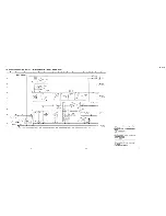
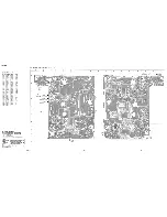
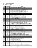
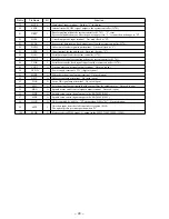
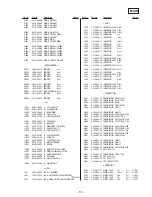
MAIN BOARD IC901 ES3210 (MPEG AUDIO/VIDEO DECODER)
Pin No.
Pin Name
I/O
Function
1
VCC
—
Power supply terminal (+3.3V)
2
DRAS B
O
Row address strobe signal output to the D-RAM (IC903) “L” active
3
DWE B
O
Write enable signal output to the D-RAM (IC903) “L” active
4 to 12
MA0 to MA8
O
Address signal output to the D-RAM (IC903)
13 to 28
DBUS0 to
DBUS15
I/O
Two-way data bus with the D-RAM (IC903)
29
RESET B
I
Reset signal input from the system controller (IC701) “L”: reset
30
VSS
—
Ground terminal
31
VCC
—
Power supply terminal (+3.3V)
32 to 39
YUV0 to YUV7
O
Video data output to the video encoder (IC920)
(YUV; Y: luminance signal, UV: Screen video interface chrominance data bus)
40
VSSCN B
O
Vertical synchronous signal output to the video encoder (IC920)
41
HSSCN B
O
Horizontal synchronous signal output to the video encoder (IC920)
42
CLK
I
System clock signal input terminal Not used (open)
43
PCLK2XSCN
I
System clock signal (27 MHz) input from the video encoder (IC920)
44
PCKLQSCN
O
Pixel clock qualifier output for the screen video interface Not used (open)
45
AUX0
O
Sub control signal output terminal Not used (open)
46
AUX1
I
Serial data input from the system controller (IC701)
47
AUX2
O
Serial data output to the system controller (IC701)
48
AUX3
O
NTSC/PAL mode selection signal output to the video encoder (IC920)
“L”: NTSC, “H”: PAL
49
AUX4
O
Sub control signal output terminal Not used (open)
50
VSS
—
Ground terminal
51
VCC
—
Power supply terminal (+3.3V)
52
AUX6
O
Communication request signal output to the system controller (IC701)
53
AUX5
I
Ready signal input from the system controller (IC701)
54
AUX7
I
Communication request signal input from the system controller (IC701)
55 to 62
LD0 to LD7
I
Data input from the program ROM (IC902)
63
LWR B
O
Write enable signal output terminal “L” active Not used (open)
64
LOE B
O
Output enable signal output to the program ROM (IC902) “L” active
65
LCS3 B
O
Chip select signal output to the program ROM (IC902) “L” active
66
LCS1 B
I
Serial data transfer clock signal input from the system controller (IC701) “L” active
67
LCS0 B
O
Chip select signal output terminal “L” active Not used (open)
68 to 79
LA0 to LA11
O
Address signal output to the program ROM (IC902)
80
VSS
—
Ground terminal
81
VPP
—
Power supply terminal (+5V) (digital system)
82 to 86
LA12 to LA16
O
Address signal output to the program ROM (IC902)
87
LA17
O
Address signal output terminal Not used (open)
88
AUDIOCLK
I
Audio master clock signal (16.9344 MHz) input from the D/A converter (IC320)
89
AOUT
O
Audio interface serial data output to the D/A converter (IC320)
90
TBCK
O
Bit clock signal (2.8224 MHz) output to the D/A converter (IC320)
91
ATFS
O
L/R sampling clock signal (44.1 kHz) output to the D/A converter (IC320)
92
DOE B
O
Output enable signal output to the D-RAM (IC903) “L” active
93
AIN
I
Audio interface serial data input terminal Not used (open)
94
RBCK
I
Audio interface bit clock signal (2.8224 MHz) input terminal Not used (open)
95
ARFS
I
Audio interface L/R sampling clock signal (44.1 kHz) input terminal Not used (open)
Summary of Contents for D-V7000
Page 4: ... 4 SECTION 2 GENERAL This section is extracted from instruction manual ...
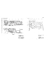
Page 10: ... 10 Connection Location CN501 CN701 MAIN Board Side A TP535 RFO TP534 VC TP524 TE ...
Page 12: ......
Page 13: ......
Page 14: ......
Page 15: ......


